An Open Engineering Project
This project began when Hadrien Theveneau shared with me the idea of developing a solid-state SP2T RF switch capable of operating from 1 to 30 MHz and carrying RF power up to 1.3 kW. When he suggested that we develop the project together, the subject immediately caught my interest.
High-power RF switching was not directly within my main area of expertise, and I initially had some hesitation for that reason. However, the problem quickly became especially interesting because it combines several engineering disciplines at once: RF, power electronics, gate drive, isolation, thermal design, and PCB parasitics. I would also like to thank Hadrien Theveneau for supporting me throughout the process, particularly by sharing his RF knowledge and experience.
From the beginning, our goal was not simply to produce a working prototype. We wanted to publish the design decisions, calculations, revisions, and test results openly, including approaches that were later changed or found to be insufficient. In engineering, the reason a design changes can often be more instructive than the final version itself.
This first part focuses on Design 1: why the initial topology was selected, which requirements drove the component choices, and which assumption had to be reconsidered during the intermediate design review.
The basic question was simple:
How can a 1–30 MHz, 1.3 kW RF signal be switched in solid state while maintaining low loss, sufficient isolation, and reliable control?
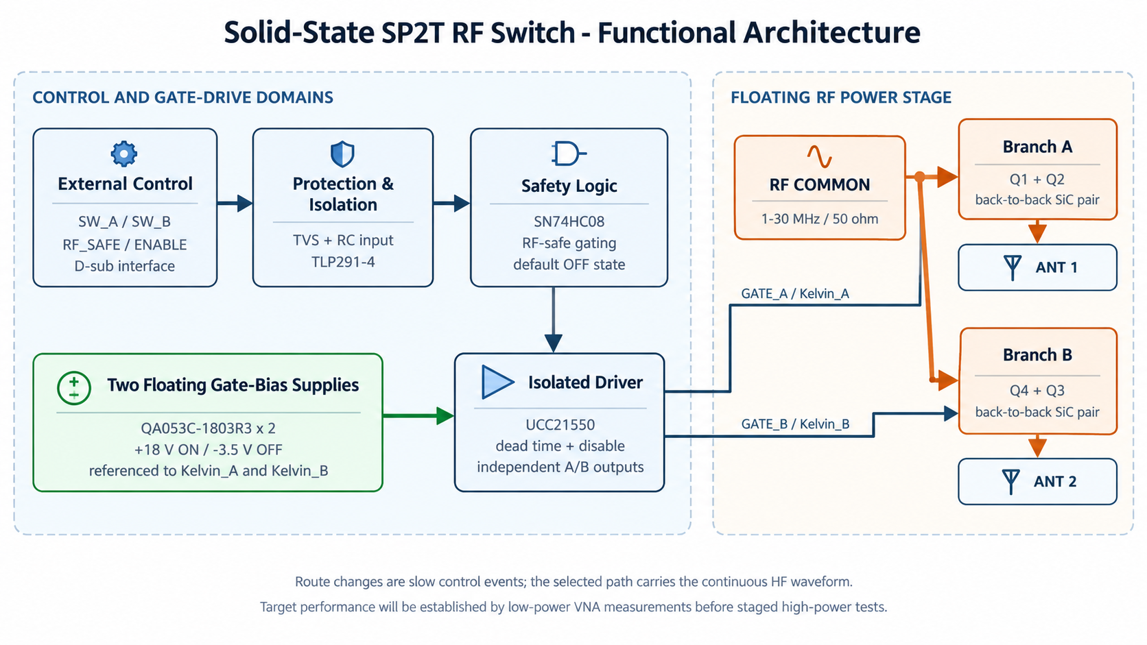
Figure 1. Design 1 functional architecture. Route selection is a slow control event; the selected branch carries the continuous HF waveform. The two RF outputs are shown as ANT 1 and ANT 2.
1. Design 1: Why Back-to-Back MOSFETs?
During the first design discussions, Hadrien Theveneau proposed using two source-to-source back-to-back N-channel MOSFETs in each RF branch.
When a single MOSFET is turned OFF, its channel stops conducting, but its intrinsic body diode still provides a conduction path in one direction. Because the RF signal is alternating, a single MOSFET cannot reliably block both polarities. Two source-to-source MOSFETs provide bidirectional conduction when ON, while their oppositely oriented body diodes block the direct conduction path when both devices are OFF.
The two-branch SP2T structure therefore requires four MOSFETs in total:
This topology was a reasonable starting point for Design 1 because it provides bidirectional RF switching without mechanical contacts. However, at 1.3 kW and up to 30 MHz, voltage rating alone was not enough. ON-state loss, OFF-state coupling, thermal behaviour, and gate-drive integrity all had to be considered together.
2. MOSFET Selection: VDS, ID, RDS(on), and OFF-State Capacitance
At 1.3 kW into a matched 50 Ω load, the nominal line values are approximately:
These are nominal matched-load values. Antenna mismatch and standing-wave conditions can increase the instantaneous voltage or current stress seen by the MOSFETs.
For that reason, four parameters became particularly important in device selection:
- VDS — sufficient voltage margin in the OFF state and under mismatch conditions,
- ID — the ability to carry the RF current and possible current peaks safely,
- RDS(on) — ON-state insertion loss and thermal dissipation,
- Coss / effective Coff — the capacitive RF path that remains toward the unselected port in the OFF state.
RDS(on) directly affects conduction loss:
This makes low RDS(on) desirable. But in an RF switch, good ON-state performance alone is not sufficient.
When the MOSFET is OFF, the channel is closed, but the drain-source path does not become an ideal open circuit. The device output capacitance, together with other topology parasitics, creates an effective OFF-state capacitance (Coff). From an RF perspective:
so the impedance of the OFF path decreases as frequency increases.
This creates an important trade-off. A larger die area may reduce RDS(on), but it often comes with higher capacitance. In other words, improving insertion loss can make port isolation more difficult.
For Design 1, the Infineon IMZC140R029M2H was selected because it combined a 1400 V class rating, the required current capability, low RDS(on), relatively low Coss, and a TO-247-4 package with a Kelvin Source connection.
Assuming approximately 58 mΩ total channel resistance for the two series MOSFETs:
The ON-state result looked promising. The later design review, however, showed that the dominant limitation could instead be OFF-state capacitance and port isolation.
Detailed RF, isolation, and thermal calculations are available here: RF & Thermal Calculation Model.
3. MOSFET Gate-Drive Architecture
After selecting the MOSFET, the next question was not simply how to turn it ON and OFF, but how to apply the correct gate-source voltage with low impedance and with a stable source reference.
Although the control side operates at approximately 5 V logic, directly driving the SiC MOSFET from an MCU GPIO would not be appropriate. A MOSFET gate draws very little DC current in steady state, but during switching its capacitances require a finite amount of charge to be moved:
For the IMZC140R029M2H, the manufacturer characterizes the gate charge using an 18 V gate-drive condition. Here it is important to distinguish threshold voltage from full enhancement: the point at which the channel starts to conduct is not the same as the operating point where the device reaches low RDS(on).
For this reason, Design 1 uses approximately +18 V ON bias.
The Miller plateau is particularly important during the gate transition. While the drain voltage is changing, a significant part of the driver current is used to transfer gate-drain charge. If the driver impedance is too high or the available gate current is too low, the transition becomes longer and the MOSFET spends more time in its intermediate region.
There is an important distinction in this project:
The RF frequency and the MOSFET switching frequency are not the same thing.
At 30 MHz, one RF period is only:
but the MOSFET gates are not being switched every 33 ns. Once a branch is selected, the MOSFETs may remain in the same ON or OFF state for seconds, minutes, or longer, while the continuous 1–30 MHz RF carrier propagates through that static conduction path.
Therefore, the reason for using a capable gate driver is not to switch the gates at 30 MHz. The gate driver is needed only during branch transitions, when it must move the gate charge in a controlled way. At the same time, parameters such as RDS(on), Coss/Coff, package inductance, and PCB parasitics directly affect RF performance because the devices continuously experience the 1–30 MHz waveform.
This distinction is central to the design: a low control switching rate limits switching losses, but it does not remove the 30 MHz OFF-state capacitance and RF isolation problem.
For this reason, a Texas Instruments UCC21550 was placed between the logic and power stages. Its two isolated channels, approximately 4 A peak source / 6 A peak sink capability, disable input, and programmable dead time are used to control route-change transients and keep the gate in a well-defined low-impedance state.
Negative OFF Bias
Instead of relying only on 0 V in the OFF state, Design 1 uses approximately −3 to −3.5 V negative gate bias.
Fast drain-voltage changes can couple displacement current into the gate through the gate-drain capacitance:
This current can create a positive voltage excursion across the gate impedance and increase the risk of false turn-on. Negative OFF bias provides additional margin below threshold and therefore improves immunity to this mechanism.
Each floating gate-drive domain is powered by a MORNSUN QA053C-1803R3 isolated bipolar DC/DC converter, providing approximately +18 V / −3.5 V gate supply rails.
Kelvin Source
Gate voltage is meaningful relative to the MOSFET source terminal, not to system ground:
Parasitic inductance in the power-source path can generate:
If the gate-driver return shares the same high-current source path, this voltage directly modulates the actual VGS seen by the MOSFET.
The Kelvin Source terminal in the TO-247-4 package is intended to separate the gate-driver return path from the main power-current path and reduce the influence of common-source inductance.
That is why Kelvin referencing was considered important in Design 1: generating +18 V or −3.5 V is not sufficient by itself; those voltages must also be applied relative to the correct source reference.
4. RF Detector and Safe Branch Switching
Sending an OFF command to one branch does not guarantee that the RF energy on that path has already fallen to a sufficiently low level. Coss, PCB parasitics, connector coupling, and transients can leave measurable RF energy at the unselected port.
For this reason, Design 1 includes an RF detector input that can monitor the actual RF state independently from the digital control state. The goal is to support break-before-make operation:
Selected branch OFF
        ↓
RF level verified as sufficiently low
        ↓
Second branch ON
Even a short interval in which both branches conduct can create severe mismatch, reflected power, and semiconductor stress. The detector path is therefore intended not only as a test feature, but also as an independent verification layer.
The same measurement path may later be useful for forward power, reflected power, and unselected-port leakage measurements.
5. Control Inputs, Isolation, and RF Connectors
External enable, branch-select, and detector signals are not connected directly to the control ground. Because long external cables can carry common-mode noise, ground-loop current, and RF coupling, the inputs are isolated through a TLP291-4 optocoupler.
The isolated signals are then passed through an SN74HC08 AND gate for logic conditioning. The purpose is to allow the driver to become active only when the required conditions are met and to reduce the risk of an invalid command reaching the power stage during startup, reset, or undefined GPIO states.
For low-speed control wiring, the design favours short connections, a controlled return path, and twisted-pair or shielded cable where appropriate. On the RF side, the 50 Ω path is maintained while power-handling capability, mechanical robustness, availability, and cost are considered together.
Schematic and component details for this section: Design 1 Schematic · BOM
6. Intermediate Design Review
After the basic Design 1 architecture was completed, Hadrien Theveneau and I carried out an intermediate design review. The goal was not simply to ask whether the circuit could work, but which assumptions were actually reliable under the 1–30 MHz and 1.3 kW targets.
The initial architecture looked consistent in several respects: the back-to-back MOSFET arrangement provided bidirectional blocking, the gate-drive architecture was defined, negative OFF bias reduced false turn-on risk, and the control side was kept galvanically isolated.
The most critical question, however, became OFF-state isolation.
When the MOSFET is OFF, the drain-source path is not an ideal open circuit. In addition to Coss, PCB parasitics, heatsink coupling, connector geometry, and floating-node behaviour can all contribute to RF appearing at the unselected port.
Because capacitive impedance falls as frequency rises, we reconsidered the assumption that a high-voltage SiC MOSFET with relatively low Coss would by itself provide sufficient isolation near 30 MHz. Coss also does not behave like a fixed linear capacitor; its real behaviour must be considered together with voltage-dependent capacitance and charge characteristics.
For this reason, Design 1 was not sent directly to PCB fabrication.
Instead, the RF switching topology was reopened for comparison with alternative approaches. Design 1 therefore became less of a discarded concept and more of a reference architecture that clearly identified the problem the next design must solve.
7. Conclusion and Next Design Direction
The main lesson from Design 1 is that, in high-power HF switching, focusing only on low RDS(on) and high VDS is not enough. OFF-state capacitance and parasitic coupling must be addressed at the topology level.
The next design work is therefore examining three main directions:
- series/shunt MOSFET topologies, including the use of shunt MOSFETs to suppress the unselected port more effectively,
- alternative MOSFETs that accept somewhat higher RDS(on) in exchange for lower Coss/Coff,
- high-voltage PIN-diode approaches intended for HF kilowatt-level switching.
At this point, the problem is no longer simply “Which MOSFET is better?”
Which switching topology provides the best balance of isolation, insertion loss, thermal performance, and circuit complexity from 1 to 30 MHz at 1.3 kW?
New topologies, updated calculations, and schematic revisions will be published in this series as the project develops. Technical comments are especially welcome on Coss modelling, shunt topology, high-power PIN-diode switching, RF isolation, and measurement strategy.
Design Files
References
-
Infineon Technologies, IMZC140R029M2H — CoolSiC™ 1400 V SiC MOSFET G2, datasheet.
https://www.infineon.com/assets/row/public/documents/60/49/infineon-imzc140r029m2h-datasheet-en.pdf -
Texas Instruments, UCC21550 — 4-A/6-A Reinforced Isolation Dual-Channel Gate Driver, datasheet.
https://www.ti.com/lit/ds/symlink/ucc21550.pdf -
Infineon Technologies, CoolSiC™ 1200 V SiC MOSFET — Application Note, especially the gate-driver design guidelines, Kelvin-source connection and parasitic turn-on considerations.
https://www.infineon.com/dgdl/Infineon-CoolSiC_MOSFET_1200V-SiC_trench_power_device-ApplicationNotes-v01_01-EN.pdf -
Infineon Technologies, Guidelines for CoolSiC™ MOSFET Gate Drive Voltage Window — AN2018-09.
https://www.infineon.com/assets/row/public/documents/cross-divisions/42/infineon-guidelines-for-coolsic-mosfet-gate-drive-voltage-window-applicationnotes-en.pdf -
Infineon Technologies, The Simplicity of Driving CoolSiC™ MOSFETs: A Gate Driving Design Guide — Miller coupling, parasitic turn-on and gate-voltage selection.
https://www.infineon.com/assets/row/public/documents/60/54/infineon-driving-coolsic-mosfets-article-en.pdf -
Texas Instruments, dV/dt Induced Turn-On and Miller-Current Considerations, application brief.
https://www.ti.com/document-viewer/lit/html/SBAA697
Status note: Design 1 is an engineering baseline, not a validated 1.3 kW product. Full-power performance remains subject to RF characterization, thermal measurements, mismatch testing and protection verification.