Part I – Gate Voltage, Gate Capacitance, Gate Charge and Miller Effect
1.1 Introduction
Anyone working in the field of power electronics will eventually encounter terms such as Qg, QGD, Ciss, Crss, Miller Plateau, dv/dt, and Gate Drivers. Although these parameters are included in almost every MOSFET datasheet, the relationships between them are often not explained in a clear and practical manner. As a result, they can easily be misunderstood or misinterpreted during the design process.
The performance of a power MOSFET is not determined solely by its RDS(on) or maximum current rating. In high-frequency switching applications, the dynamic behavior of the gate has a direct impact on switching speed, power losses, electromagnetic interference (EMI), and ultimately the overall reliability of the system. For this reason, understanding the fundamental principles of gate driving is an essential part of designing efficient and reliable power electronic systems.
The primary objective of this guide is to bring together the information scattered across manufacturers’ application notes and datasheets into a single document, presenting these concepts in a logical sequence with a practical design perspective. Rather than explaining the internal structure or complete operating principles of MOSFETs, this guide focuses on the key concepts that govern gate drive behavior and their impact on switching performance.
Since the subject of gate driving is extensive, this guide has been organized into two parts. Part I introduces the fundamental concepts, including gate voltage limits, gate capacitances, Gate Charge, Miller Effect, and their influence on switching behavior. Part II builds upon this theoretical foundation by covering practical gate driver circuits, different driving techniques, PCB layout considerations, and design-oriented interpretation of MOSFET datasheets.
It is my hope that this guide will serve as a practical reference for engineers working in power electronics, as well as for students interested in the subject, helping them develop a more comprehensive understanding of MOSFET gate driving principles.
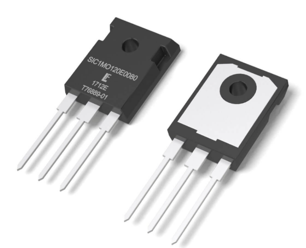
Figure 1: Various types of MOSFET packages used in modern electronics
1.2 Why Was This Guide Prepared?
A MOSFET datasheet contains many parameters, including Qg, Qgd, Ciss, Crss, Miller Plateau, dv/dt, and gate driver current. Although each parameter may appear understandable on its own, incorrect design decisions can result when the relationships between them are not properly established.
For example:
- Why can a MOSFET with a low RDS(on) still experience high power dissipation?
- Why does the same gate driver produce different switching times with different MOSFETs?
- Why is it not sufficient to select a MOSFET based only on its total Qg value?
- Why does the Miller Plateau occur, and why is it important?
This guide aims to answer these questions from a practical, design-oriented perspective.
Designer’s Note
Many problems encountered in power electronics are caused not by the static characteristics of the MOSFET, but by its dynamic switching behavior. A proper understanding of the switching process is therefore essential for designing efficient, reliable, and predictable power electronic systems.
1.3 What Will You Find in This Guide?
This guide examines the following topics step by step:
- Gate voltage limits
- Standard-level and logic-level MOSFETs
- Gate capacitances: CGS, CGD, and CDS
- The meaning of Ciss, Coss, and Crss
- Gate Charge (Qg) and gate current
- Miller Effect and Miller Plateau
- The influence of gate-related parameters on switching behavior
- Practical datasheet interpretation and design considerations
Each section includes not only theoretical explanations, but also practical design notes and common mistakes encountered during MOSFET gate-drive design.
1.4 Structure of the Guide
This guide is organized to progress from the fundamental gate-related characteristics of a power MOSFET toward their practical impact on switching behavior.
Part I focuses on gate voltage limits, input capacitances, Gate Charge, Miller Effect, and Miller Plateau. These topics establish the theoretical foundation required to understand how a MOSFET responds to a gate-drive signal.
Part II will build on this foundation by examining gate driver design, ground-referenced and floating driver circuits, PCB layout considerations, and the design-oriented interpretation of MOSFET datasheets.
The objective of this two-part structure is to first explain the physical and electrical behavior of the MOSFET gate, and then demonstrate how this knowledge can be applied in practical gate-driver design.
![Figure 2 Gate Voltage Limits Source [1]](/images/articles/power-mosfet-gate-drive-fundamentals-1-2/figure-02.png)
Figure 2 Gate Voltage Limits Source [1]
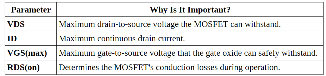
2.3 Key Datasheet Parameters
A typical MOSFET datasheet contains dozens of electrical parameters. However, for an initial device evaluation, the following four parameters are sufficient in most applications.
Designer’s Note
When selecting a MOSFET, RDS(on) should never be considered in isolation. The drain-to-source voltage rating (VDS), the recommended gate drive voltage, and the intended operating conditions should always be evaluated together.
✔ Key Takeaways
- The gate oxide is the most voltage-sensitive part of a MOSFET.
- VGS(max) is an absolute maximum rating, not the recommended operating voltage.
- VGS(th) does not represent the voltage required for full conduction.
- The RDS(on) test conditions provide more meaningful information than the threshold voltage when selecting a MOSFET.
- During the initial selection process, VDS, ID, VGS(max), and RDS(on) should always be evaluated together.
CHAPTER 3
Gate Input Characteristics
3.1 Static and Dynamic Gate Behavior
The behavior of a MOSFET gate can be analyzed under two different operating conditions.
Static (Steady-State) Operation
When the MOSFET is fully ON or fully OFF, only a negligible leakage current flows into the gate terminal. Consequently, the gate driver consumes virtually no steady-state power.
Dynamic (Switching) Operation
The situation changes during switching. The energy supplied by the gate driver is used to charge and discharge the MOSFET’s internal gate capacitances. As a result, the current capability of the gate driver directly determines how quickly the MOSFET can turn on and off.
Designer’s Note
The statement “A MOSFET gate does not draw current” is only valid under steady-state conditions. During switching, a significant gate current flows while charging and discharging the gate capacitances. This transient current is one of the key factors determining the overall performance of the gate driver.
![Figure 3 MOSFET gate capacitances Source [1]](/images/articles/power-mosfet-gate-drive-fundamentals-1-2/figure-04.png)
Figure 3 MOSFET gate capacitances Source [1]
3.2 Gate Capacitances
The gate terminal of a MOSFET cannot be represented by a single capacitor. Instead, the device contains three fundamental parasitic capacitances that are commonly defined in manufacturers’ datasheets:
- Gate-to-Source Capacitance (CGS)
- Gate-to-Drain Capacitance (CGD)
- Drain-to-Source Capacitance (CDS)
These capacitances originate from the physical structure of the MOSFET and have a direct influence on its switching behavior.
Among them, CGD is particularly important because it couples changes in the drain voltage to the gate terminal, making it the primary cause of the Miller Effect.
Designer’s Note
While CGS primarily influences the initial turn-on behavior of the MOSFET, CGD is one of the most critical capacitances affecting switching speed and electromagnetic interference (EMI). In high-frequency applications, designers should consider not only the total Gate Charge, but also CGD and its corresponding datasheet parameter, Crss.
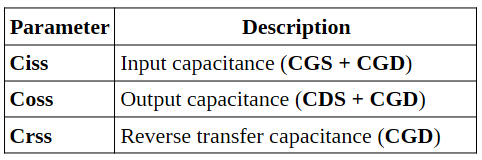
3.3 Why Do Datasheets Specify Ciss, Coss, and Crss Instead of CGS, CGD, and CDS?
Rather than specifying CGS, CGD, and CDS individually, MOSFET datasheets typically provide the following equivalent capacitances.
3.4 Gate Capacitances Are Not Constant
Although MOSFET datasheets present capacitance values as fixed numerical parameters, these capacitances are not constant. In particular, the Gate-to-Drain capacitance (CGD) varies significantly with the Drain-to-Source voltage (VDS).
As VDS decreases, CGD increases. This variation directly affects the load seen by the gate driver during switching and plays a major role in the formation of the Miller Plateau.
For this reason, designers should not rely solely on the capacitance values listed in the datasheet tables. The Capacitance vs. VDS characteristic curves should also be examined, especially in high-frequency switching applications.
![Figure 4 E xample of capacitance between terminals as well as capacitance vs. drain to source voltagecharacteristics. Source [2]](/images/articles/power-mosfet-gate-drive-fundamentals-1-2/figure-06.png)
Figure 4 E xample of capacitance between terminals as well as capacitance vs. drain to source voltagecharacteristics. Source [2]
CHAPTER 4
Gate Charge and Gate Driver Design
4.1 Why Is the Gate Charge Concept Necessary?
In the previous chapter, it was explained that the gate terminal of a MOSFET is not an ideal input, but consists of three fundamental parasitic capacitances: CGS, CGD, and CDS. At first glance, it may seem that these capacitances alone are sufficient to estimate the switching behavior of the device. In practice, however, this assumption is not accurate.
The input capacitances of a MOSFET are not constant during operation. In particular, the Gate-to-Drain capacitance (CGD) varies significantly with the Drain-to-Source voltage (VDS). As a result, neither the energy required from the gate driver nor the switching time can be accurately determined by considering the Ciss value alone.
For this reason, MOSFET manufacturers use the Gate Charge (Qg) parameter, which represents the total amount of charge that must be delivered to the gate during the switching process, rather than relying solely on capacitance values.
![Figure 5 Gate Charge Measurement Circuit Soruce [2]](/images/articles/power-mosfet-gate-drive-fundamentals-1-2/figure-07.png)
Figure 5 Gate Charge Measurement Circuit Soruce [2]
Designer’s Note
Since the MOSFET gate exhibits capacitive behavior, the gate driver does more than simply provide a voltage. Its primary function is to deliver the required gate charge as quickly as possible, enabling the MOSFET to switch efficiently.
4.2 What Is Gate Charge (Qg)?
Gate Charge (Qg) is the total amount of electrical charge that must be delivered to the MOSFET gate in order to fully turn the device on under specified operating conditions. It is expressed in nanocoulombs (nC) and is one of the most important parameters for evaluating the dynamic performance of a MOSFET.
Unlike Ciss, Gate Charge is not a capacitance. Instead, it is an experimentally measured parameter that represents the combined switching behavior of all the gate-related capacitances during the turn-on process.
For this reason, in high-frequency power electronic applications, MOSFET selection should not be based solely on the Ciss value. The Gate Charge (Qg) should also be carefully evaluated, as it directly influences the required gate drive capability and the achievable switching performance.
![Figure 6 VGS against QG under different VGS and ID conditions Source [1]](/images/articles/power-mosfet-gate-drive-fundamentals-1-2/figure-08.png)
Figure 6 VGS against QG under different VGS and ID conditions Source [1]
4.3 How to Interpret the Gate Charge Curve
A typical Gate Charge curve shows that the gate voltage does not increase linearly during the switching process. This is because switching consists of several distinct physical events rather than a single continuous charging process.
The Gate Charge curve can be divided into three main regions:
- QGS – The region where the Gate-to-Source capacitance is charged and the conductive channel begins to form.
- QGD – The region during which the drain voltage changes. This interval is commonly referred to as the Miller Plateau.
- Qg – The total gate charge required to fully turn the MOSFET on.
The physical significance of these regions and their impact on switching performance will be discussed in detail in the next chapter.
Note: This section introduces only the overall structure of the Gate Charge curve. The concepts of QGS, QGD, and the Miller Plateau are explained in detail in Chapter 5.
4.4 Why Is Gate Charge Important?
Two MOSFETs may have identical RDS(on) values while exhibiting completely different Gate Charge (Qg) values. As a result, the same gate driver can produce significantly different switching times.
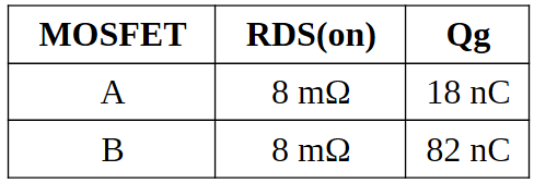
Although both devices have similar conduction losses, the MOSFET with a Gate Charge of 82 nC requires considerably more gate current to achieve the same switching speed.
Therefore, a higher Qg is not necessarily a disadvantage. It should always be evaluated together with the current capability of the selected gate driver and the switching requirements of the application.
⚠️ Common Mistake
Incorrect assumption
A MOSFET with a lower Qg is always the better choice.
Correct approach
Qg is only one of the parameters affecting switching performance. Although a lower Qg generally enables faster switching, it should always be evaluated together with RDS(on), thermal performance, switching frequency, and the overall application requirements.
✔ Key Takeaways
- Gate Charge (Qg) is the total electrical charge that must be delivered to the gate to fully turn the MOSFET on.
- Qg is a more meaningful parameter than capacitance alone when evaluating dynamic switching performance.
- MOSFETs with identical RDS(on) values may have significantly different Qg values.
- A typical Gate Charge curve consists of the QGS, QGD, and Qg regions.
- The next chapter explains how these regions are related to the Miller Effect and the Miller Plateau.
CHAPTER 5
Miller Effect and Switching Dynamics
5.1 What Is the Miller Effect?
One of the most important parasitic elements affecting MOSFET switching performance is the Gate-to-Drain capacitance (CGD). This capacitance provides an electrical coupling between the gate and drain terminals, allowing changes in the drain voltage to influence the gate voltage. This phenomenon is known as the Miller Effect.
During switching, the energy supplied by the gate driver is not used solely to increase the gate voltage. During a certain portion of the switching process, a significant part of this energy is used to charge the Gate-to-Drain capacitance. As a result, the gate voltage temporarily remains almost constant, forming the characteristic region known as the Miller Plateau.
5.2 What Actually Happens When a MOSFET Turns On?
When a gate driver begins turning on a MOSFET, the gate current does not charge the entire gate structure instantaneously. Instead, the switching process occurs in several distinct stages.
Stage 1 – Initial Charging of the Gate Capacitances
As the gate driver starts supplying current, the gate current initially charges the CGS capacitance. During this period, VGS increases while virtually no drain current flows.
Stage 2 – Channel Formation
Once the gate voltage reaches the threshold voltage (VGS(th)), the conductive channel begins to form and the drain current starts to increase. However, the MOSFET has not yet reached full conduction.
Stage 3 – Miller Region
After the drain current reaches the load current, the Drain-to-Source voltage (VDS) begins to decrease. At this point, a large portion of the energy supplied by the gate driver is used to charge the CGD capacitance.
Consequently, the gate voltage remains nearly constant for a short period. This constant-voltage interval is known as the Miller Plateau.
![Figure 7: MOSFET gate charge, drain voltage and current during switch-on(ideal waveforms) Source [1]](/images/articles/power-mosfet-gate-drive-fundamentals-1-2/figure-10.png)
Figure 7: MOSFET gate charge, drain voltage and current during switch-on(ideal waveforms) Source [1]
Figure Description: During t₀–t₁, the gate capacitances are charged and VGS begins to rise. Between t₁ and t₂, the conductive channel is established, allowing the drain current to increase. The interval from t₂ to t₃ represents the Miller Plateau, where VDS falls rapidly while VGS remains nearly constant as the CGD capacitance is being charged. Finally, during t₃–t₄, the MOSFET reaches full enhancement and VGS rises to its final drive voltage.
5.3 How Is the Miller Plateau Identified in a Datasheet?
The Miller Plateau is not merely a theoretical concept. It can be clearly observed on the Gate Charge curve provided in MOSFET datasheets.
Designer’s Note
Two MOSFETs may have the same total Qg while exhibiting different QGD values. A device with a lower QGD can complete the Miller interval more quickly and may therefore achieve lower switching losses in high-frequency applications.
For this reason, MOSFET selection should not be based on total Qg alone.
5.4 Miller Plateau and Switching Losses
The highest switching losses generally occur during the Miller Plateau because the MOSFET simultaneously carries:
- High drain current, ID
- High drain-to-source voltage, VDS
The switching loss can be approximately estimated as:
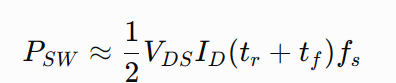
where:
- tr is the rise time,
- tf is the fall time,
- fs is the switching frequency.
As the duration of the Miller Plateau increases, the effective switching transition times also increase. Consequently, switching losses rise and the MOSFET dissipates more heat.
5.5 Why Does the Miller Plateau Voltage Change?
The Miller Plateau does not occur at a fixed gate voltage. Its level depends on both the MOSFET characteristics and the operating conditions.
During this interval, the gate voltage is associated not only with the charging of the internal capacitances, but also with the drain current being conducted. As the load current increases, a higher VGS is generally required to support that current. Therefore, the Miller Plateau voltage tends to rise at higher drain currents.
The plateau voltage may also differ between MOSFETs because of variations in transconductance, gfs and device structure. As a result, two MOSFETs driven by the same gate voltage may exhibit different Miller Plateau levels.
Designer’s Note
The Miller Plateau voltage shown in a datasheet is valid only for the specified test conditions. Changes in drain current, bus voltage, temperature, or circuit conditions may shift both the plateau voltage and its duration.
✔ Design Considerations
- Do not evaluate a MOSFET using total Qg alone.
- A higher QGD may result in longer switching transitions and greater switching losses.
- A gate driver with sufficient current capability can reduce the duration of the Miller interval.
- Increasing the gate resistance generally extends the Miller Plateau duration.
- PCB parasitic inductance may worsen gate ringing and increase the risk of unintended switching.
5.6 Why Should the Miller Region Be Crossed Quickly?
During the Miller Plateau, the MOSFET is exposed to both a significant VDS and a high ID. Therefore, a large portion of the switching loss is generated during this interval.
As the current capability of the gate driver increases, the CGD capacitance can be charged more quickly and the duration of the Miller Plateau is reduced. The MOSFET then reaches full conduction in a shorter time, lowering switching losses.
For this reason, providing the correct gate voltage alone is not sufficient in high-frequency power converters. The gate driver must also provide adequate source and sink current.
Designer’s Note
MOSFETs with a high total Qg require a higher gate-driver current to achieve the same switching speed.
5.7 Design Implications of the Miller Effect
The Miller Effect influences more than switching losses. In an improperly designed gate-drive circuit, it may also lead to:
- Longer switching transitions
- Increased EMI
- Gate-voltage overshoot and ringing
- Unintended turn-on in half-bridge circuits
- Shoot-through current
At high dv/dt, current coupled through CGD may raise the gate voltage of a MOSFET that is intended to remain off. In half-bridge and full-bridge topologies, this can create serious reliability problems.
⚠️ Common Mistake
Reducing the gate resistance as much as possible is not always the best approach. Although a smaller gate resistance increases switching speed, it also increases dv/dt, ringing, and the risk of Miller-induced false turn-on.
Conclusion
This study examined the fundamental electrical and dynamic characteristics that determine the gate-drive behavior of power MOSFETs. First, gate-voltage limits and suitable gate-drive levels were discussed. The internal capacitances of the MOSFET—CGS, CGD, and CDS—were then introduced, together with their corresponding datasheet parameters, Ciss, Coss, and Crss.
The concept of Gate Charge (Qg) was subsequently explained, along with the relationship between gate charge and switching performance. Finally, the Miller Effect and Miller Plateau were examined, with particular emphasis on their influence on switching time, switching losses, and gate-driver requirements.
The main purpose of this guide is to explain the fundamental concepts governing power MOSFET gate-drive dynamics in a clear and application-oriented manner. This foundation is intended to help designers interpret the dynamic parameters presented in MOSFET datasheets more accurately and make better-informed engineering decisions when developing gate-drive circuits.
This document forms Part I of the Power MOSFET Gate Drive Fundamentals series. Part II will build on the principles introduced here and will cover gate-driver design, ground-referenced drivers, floating drivers, PCB layout considerations, and the design-oriented interpretation of MOSFET datasheets. The objective is to show how the theoretical concepts discussed in this first part can be applied in practical power-electronics designs.
References
[1] Infineon Technologies, Gate Drive for Power MOSFETs in Switching Applications – A Guide to Device Characteristics and Gate Drive Techniques, Application Note, Rev. 1.1, 2022. Available: https://www.infineon.com/assets/row/public/documents/24/42/infineon-gate-drive-for-power-mosfets-in-switchtin-applications-applicationnotes-en.pdf
[2] Renesas Electronics, Power MOSFET Application Note. Available: https://www.renesas.com/us/en/document/apn/power-mosfet-application-note
[3] Texas Instruments, AN-558: Introduction to Power MOSFETs and Their Applications (SNVA008). Available: https://www.ti.com/lit/an/snva008/snva008.pdf
[4] B. J. Baliga, Fundamentals of Power Semiconductor Devices, 2nd ed. Cham, Switzerland: Springer, 2019.
[5] M. H. Rashid, Power Electronics: Circuits, Devices, and Applications, 4th ed. Pearson, 2014.
The concepts and examples presented in this guide are based on application notes published by leading semiconductor manufacturers and widely accepted references in the field of power electronics.