Study scope: This article reports LTspice simulations and circuit analysis. It does not report bench measurements or validated hardware performance. The figures preserve the original simulation study; supply-voltage and device-variant limitations are discussed below.
1. Introduction
Peak detector circuits, which I personally find to be one of the most interesting structures in analog electronic design, form the main focus of this study. In optical sensing systems, pulse-shaped signals obtained from sensors pass through filtering, amplification, and transmission stages, gradually deviating from their ideal square-wave form and transforming into more complex waveforms. Processing such high-speed signals directly often requires high-speed ADC systems and complex digital algorithms.
However, in many applications, obtaining only the maximum value of the signal reliably is sufficient instead of processing the entire waveform. Peak detector circuits provide an effective solution for this purpose. These circuits capture the highest value of the input signal, store it on a capacitor, and preserve this information until measurement is completed. As a result, transient high-speed pulses can be measured even by relatively slower measurement systems.
In this article, a conventional simplified peak detector structure is first examined, followed by a detailed analysis of active peak detector architectures developed for high-speed applications. In addition, LTspice simulations were performed to compare the behavior of different peak detector structures under varying input frequencies and voltage levels. Throughout the study, the main parameters affecting peak detector performance were investigated in order to better understand how the most suitable peak detector structure can be designed for different operating conditions.
2. Peak Detection Principles
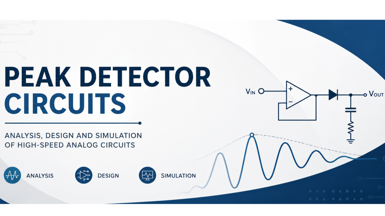
Peak detector circuits are fundamental analog processing structures that detect the maximum voltage level reached by an analog signal and store this information for a certain period of time. In systems containing short-duration pulses, directly measuring the instantaneous peak value of the signal is often difficult or impractical. Therefore, peak detector circuits serve as an interface between fast analog signals and relatively slower measurement systems. Optical sensing systems, radar applications, RF measurements, medical electronic systems, and high-speed data acquisition circuits are among the common application areas of peak detectors.
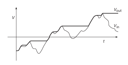
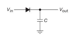
The simplest peak detector structure consists of a diode and a capacitor. When the input signal increases, the diode becomes forward biased and charges the capacitor. As the signal begins to decrease, the diode turns off and preserves the voltage stored on the capacitor. Although this structure is simple, the forward voltage drop of the diode introduces significant errors, especially for low-level signals. In addition, diode recovery time, capacitor leakage currents, and load effects can degrade peak detection performance in high-frequency pulse applications.
The limitations of passive structures have led to the development of active peak detector circuits capable of operating with higher accuracy and speed. In these circuits, an operational amplifier (op-amp) is used to compensate for the diode forward voltage drop through feedback, enabling more accurate peak detection, especially for low-level signals. A simple active peak detector without a hold-phase feedback path may drive its op-amp into saturation when the rectifier diode turns off. Recovery can then delay acquisition of the next peak. Anti-saturation feedback can reduce this problem; Figure 4 includes such a path through D1. Short-pulse accuracy still depends on charging current, settling, and the device models.
For this reason, modern peak detector designs commonly employ high-speed op-amps, Schottky diodes, local feedback structures, and sample-and-hold-like techniques. Op-amps with low input bias current, high slew-rate capability, and low input capacitance help reduce voltage loss on the hold capacitor, resulting in more accurate peak measurements.
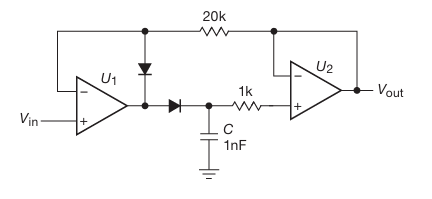
Peak detector circuits are often discussed together with sample-and-hold structures, since both systems aim to preserve analog signal information for a certain period of time. However, in sample-and-hold circuits, the storage operation is controlled by an external control signal, whereas in peak detector circuits the capacitor automatically tracks and stores the maximum value reached by the input signal. For this reason, peak detectors provide a more practical solution for detecting the maximum amplitude of short-duration transient pulses.
Based on these fundamental operating principles, the next section examines conventional and improved active peak detector architectures in detail.
3. Peak Detector Architectures
This section examines LTC6244-based peak detector circuits designed for high-speed analog signal peak detection. Conventional and improved active peak detector architectures are analyzed in terms of operating principles, dynamic behavior, and high-frequency performance limitations.
3.1 Conventional Active Peak Detector
Conventional active peak detector circuits are fundamental analog structures used to detect and store the maximum voltage level reached by an input signal on a capacitor. These circuits are widely used in applications where short-duration pulses must be measured by relatively slower measurement systems. Although this structure can provide satisfactory performance in low- and medium-frequency applications, it has several important limitations under high-speed pulse conditions.
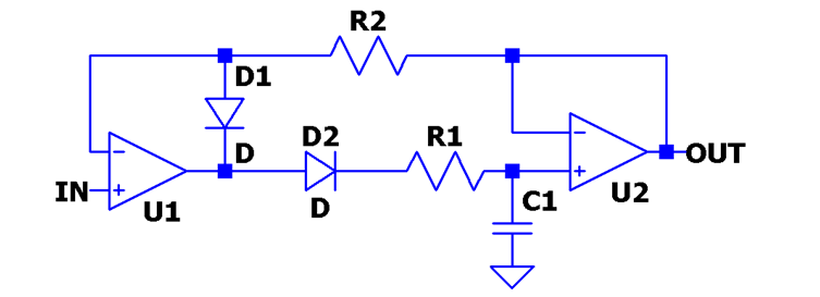
In the conventional active peak detector circuit shown in Figure 4, the U1 op-amp operates as an active rectifier. In passive peak detector circuits, the forward voltage drop of the diode, typically around 0.6–0.7 V, introduces significant measurement errors, especially for low-amplitude signals. By using an op-amp, this voltage drop is largely compensated through feedback, resulting in more accurate peak detection.
The circuit operation can generally be analyzed in two different operating modes: tracking mode and hold mode.
Tracking mode: As the input signal increases, the output of the U1 op-amp also rises, causing diode D2 to become forward biased. As a result, capacitor C1 charges while tracking the input signal. This operating region is referred to as the tracking mode. During this mode, the voltage across the capacitor represents the instantaneous peak value of the input signal.
Hold mode: When the input signal begins to decrease, diode D2 becomes reverse biased and turns off. This prevents the capacitor from discharging back into the input stage and preserves the stored peak information. This operating region is referred to as the hold mode. During the hold period, the voltage across the capacitor represents the last maximum value reached by the input signal.
The resistor R2 forms part of the feedback path of the U1 op-amp. This resistor helps maintain controlled active-diode operation and assists in compensating for the diode forward voltage drop. As a result, more accurate measurements can be achieved compared to conventional passive peak detector structures.
The resistor R1 and capacitor C1 placed after diode D2 form the RC structure that determines the main charging dynamics of the circuit. The corresponding time constant is given by:
The resistor R1 primarily limits the charging current of capacitor C1 and reduces sudden current variations at the op-amp output. This improves overall system stability and provides more controlled tracking behavior under high-frequency pulse conditions.
The RC time constant directly affects how quickly the capacitor can follow the input signal. If the RC value is too large, the capacitor cannot charge fast enough during short-duration pulses, preventing accurate peak detection. On the other hand, very small RC values allow faster response, but may increase noise sensitivity and instability.
Capacitor C1 is the main element responsible for storing the peak information. However, the voltage stored on the capacitor cannot be preserved indefinitely. Leakage current, op-amp input bias current, and load effects gradually discharge the capacitor over time. This gradual voltage reduction is commonly referred to as droop error in analog measurement systems. Especially during long hold periods, droop error becomes one of the major factors limiting measurement accuracy.
The U2 op-amp in the circuit is configured as a voltage follower. The main purpose of this stage is to isolate the hold line from the output load. If the output were connected directly to the capacitor, the measurement system connected to the output would begin discharging the capacitor and distort the stored peak voltage. By using U2, the capacitor is buffered by a high-input-impedance stage, preventing load variations from directly affecting the hold capacitor.
When D2 turns off in Figure 4, D1 provides an alternative feedback path around U1, with R2 connecting the inverting node to the buffered output. This limits the excursion of U1 during hold. The circuit should therefore not be described as an uncompensated detector whose op-amp necessarily becomes open-loop whenever D2 turns off.
If an op-amp nevertheless reaches saturation under a particular operating condition, its recovery time can delay acquisition of a new peak. Whether that occurs in these circuits needs to be checked from the op-amp output and input-node waveforms; reduced peak amplitude alone does not prove saturation.
The ability of the op-amp to follow high-speed signals is largely limited by its slew-rate capability. Slew rate defines the maximum rate of change of the op-amp output voltage with respect to time.
If the rate of change of the input signal exceeds the slew-rate capability of the operational amplifier, the output can no longer accurately track the input waveform, resulting in peak tracking error. Under these conditions, the detected peak value deviates from the actual peak amplitude of the input signal, particularly in high-frequency pulse applications.
As a consequence, conventional peak detector architectures often become insufficient for high-speed optical sensing systems, where short-duration transient signals require fast and accurate peak tracking. Therefore, more advanced peak detector structures with improved transient response and reduced recovery limitations are generally preferred in high-speed applications.
3.2 Improved Peak Detector
Figure 5 explores a different feedback and bias arrangement. Both Figure 4 and Figure 5 include feedback intended to limit op-amp excursions during hold; the comparison is therefore not simply between an open-loop hold phase and an anti-saturation design. The modified circuit also changes the diode choice, input attenuation, and output gain.
To reduce these limitations, the improved peak detector structure employs Schottky diodes, a local feedback network, and an additional biasing structure.
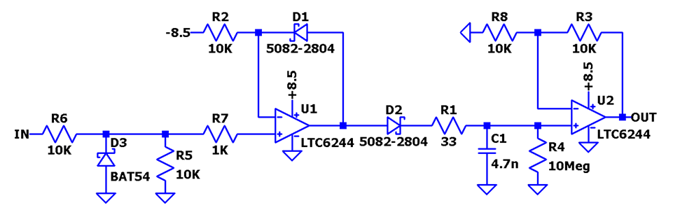
In the circuit shown in Figure 5, the first major difference compared to the conventional structure is the use of Schottky diodes as the rectifying elements. Since Schottky diodes have a lower forward voltage drop than conventional PN-junction diodes, capacitor C1 can charge more rapidly. In addition, the minority carrier storage effect in Schottky diodes is significantly lower than in conventional PN-junction diodes. In conventional diodes, the carriers stored in the junction region during conduction require a certain amount of time to be removed before the diode can fully switch off. This effect is considerably reduced in Schottky diodes. As a result, Schottky diodes exhibit much shorter reverse recovery times and faster switching behavior. This improves the transition from tracking mode to hold mode and reduces peak detection error in high-frequency pulse applications.
However, the lower forward voltage drop of Schottky diodes alone is not sufficient. In conventional peak detector structures, diode-related errors are largely compensated by the external feedback loop, whereas in this structure the voltage drop across D2 can directly appear at the output. To reduce this effect, diode D1 is added to the local feedback path of the U1 op-amp. When D1 and D2 are selected as Schottky diodes with similar characteristics, their forward voltage drops largely compensate each other, reducing diode-induced measurement errors.
The resistor R2 determines the bias current of diode D1. This structure prevents the U1 op-amp from becoming completely open-loop and allows more controlled operation. The local feedback network keeps the op-amp closer to its linear operating region and reduces recovery time effects. Especially under high-speed pulse conditions, op-amp saturation is minimized, improving transient response performance.
Resistors R5 and R6 form an input attenuator. Diode D3 provides a clamp for negative excursions, but input voltage and clamp current still need to remain within the device limits. Figure 5 also includes a −8.5 V bias connection through R2; the illustrated circuit therefore does require a negative bias source.
Supply and model limitation: Figure 5 labels the op-amps LTC6244 while showing a +8.5 V supply relative to ground. The standard LTC6244 has a recommended total supply range of 2.8–6 V and a 7 V absolute maximum; the HV variant supports a higher supply range. The figure does not identify an HV variant. Its supply and model selection must therefore be corrected and the simulation rerun before using it as a hardware design. A plausible simulation trace does not establish operation within device ratings. See the manufacturer datasheet.
Capacitor C1, charged through diode D2, stores the peak information. Resistor R1 limits the charging current of the capacitor, reducing sudden current variations and improving overall system stability. This structure also reduces abrupt current demands at the op-amp output under high dv/dt conditions. If the R1 value is selected too large, the capacitor cannot reach the true peak level during short pulses. On the other hand, excessively small R1 values may increase noise sensitivity and instability.
The U2 output stage is a non-inverting amplifier with a high-impedance input, rather than a unity-gain voltage follower. In Figure 5, R3 is the feedback resistor and R8 connects the inverting input to ground. Their equal values give a nominal voltage gain of 2, compensating for the approximately 2:1 attenuation of the input divider. This fixed gain does not, by itself, correct frequency-dependent peak-tracking error.
This structure allows the peak information to be transferred to subsequent measurement stages with improved amplitude and stability.
The LTC6244 op-amp used in the circuit provides characteristics well suited for high-speed peak detection applications. Its 50 MHz gain-bandwidth product and 40 V/μs slew-rate capability enable short-duration high-frequency pulses to be tracked with lower tracking error. In addition, the low input capacitance and rail-to-rail output structure support high-speed operation. The low input bias current helps reduce unnecessary discharge of the hold capacitor, while the low offset voltage improves overall measurement accuracy.
These changes are intended to improve acquisition and hold behavior. Whether they improve accuracy over Figure 4 must be established under matched simulation conditions; the topology alone does not guarantee better performance.
4. Simulation Results
The following LTspice simulations explore the conventional and modified peak detector circuits under the input conditions shown in each figure. Frequency, pulse duration, amplitude, and, in some runs, circuit gain were varied. These examples are not a fully controlled, point-by-point comparison under identical conditions. Here, “improved” identifies the modified topology, not a demonstrated performance advantage.
Pulse repetition frequency and pulse width are separate parameters: changing does not necessarily change repetition frequency. Both must be specified, together with rise/fall times, supply rails, load, reset timing, and the output sampling instant, for a reproducible comparison. Component designators refer to the schematic associated with each simulation and may differ between figures.
4.1 Conventional Peak Detector Simulation
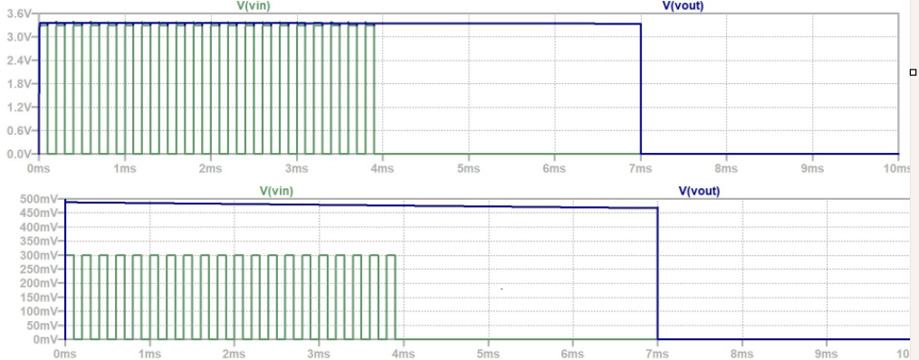
In peak detector circuits, when the input signal disappears, the voltage stored on the hold capacitor may remain from the previous measurement cycle. Under these conditions, it is not always possible to clearly determine whether the observed output voltage belongs to the new input signal or is simply residual voltage remaining from the previous measurement. In addition, when the input signal becomes active, output fluctuations may occur and the circuit may require a certain settling time before reaching a stable operating condition.
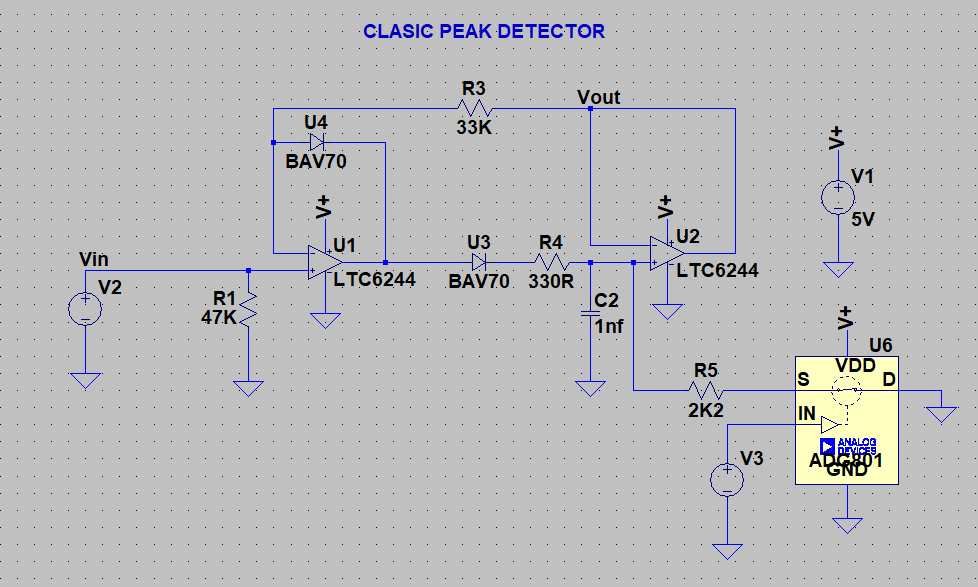
For this reason, a controlled discharge mechanism was considered necessary in order to read the peak value at the correct moment. In this study, the ADG801 analog switch was selected for this purpose. The low ON resistance, low leakage current, fast switching speed, and low charge injection characteristics of the ADG801 provide important advantages for peak detector applications. As a result, the hold capacitor can be discharged rapidly and in a controlled manner, eliminating residual voltage from previous measurements and ensuring that each measurement corresponds only to the current input signal.
In analog switch selection, parameters such as ON resistance, leakage current, switching speed, charge injection, and operating frequency are particularly important. High ON resistance or excessive charge injection can introduce distortion at the detected peak level and lead to measurement errors. Therefore, for high-frequency applications, it is critical to use low-loss and high-speed analog switches.
4.1.1 Frequency Response Simulation
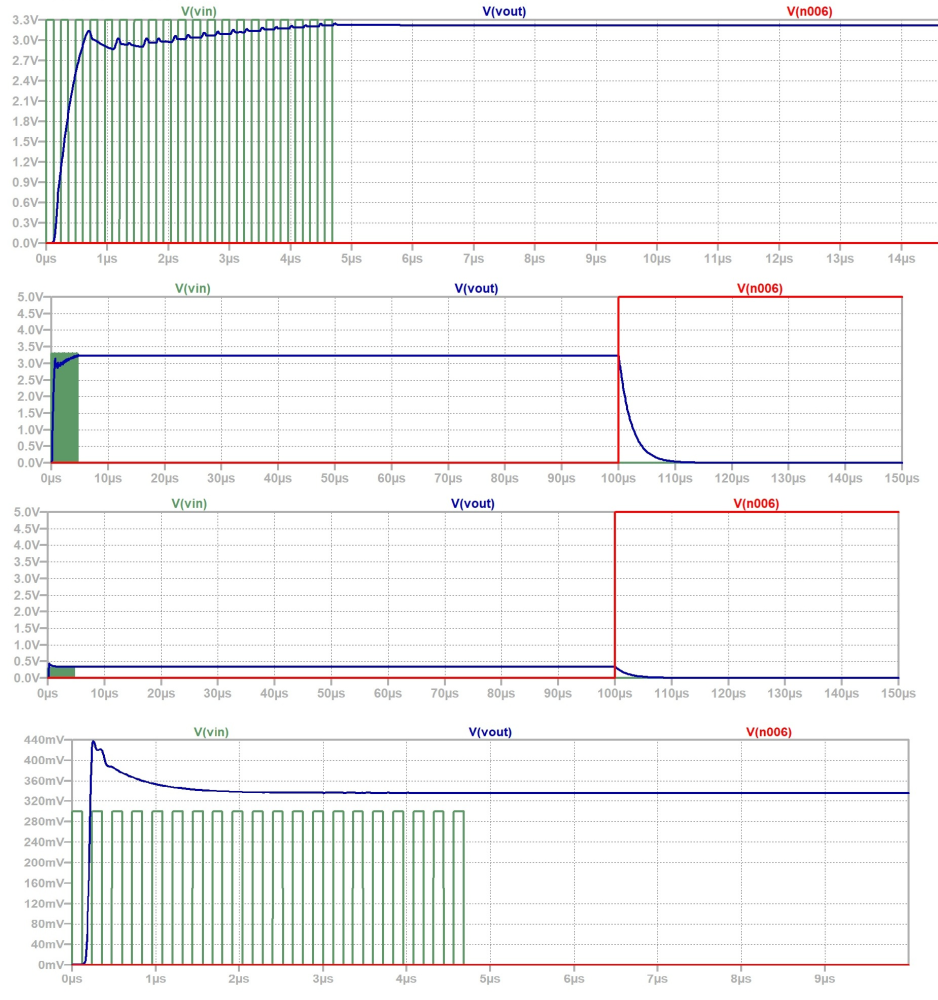
To investigate the frequency behavior of the conventional peak detector circuit, the circuit was tested under both low- and high-frequency input signals. Simulation results showed that the circuit was generally capable of tracking the peak value in both frequency regions. However, it was observed that the proper selection of the RC time constant and circuit component values becomes increasingly critical as the operating frequency changes.
The results also showed that under high-frequency pulse conditions, slight reductions in the detected peak level occurred due to op-amp slew-rate limitations, diode switching behavior, and insufficient capacitor charging. These observations indicate that peak tracking performance is strongly dependent on the capacitor charging dynamics, op-amp dynamic characteristics, and selected component values.
4.1.2 Conventional Peak Detector Under Different Input Frequencies
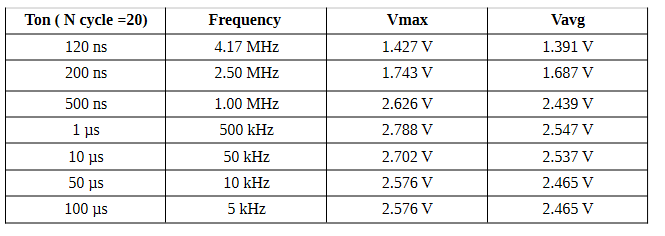
In this test, the input voltage was fixed at 2.5 V while different durations were applied in order to investigate the frequency response of the circuit. According to the simulation results, the circuit exhibited its best peak tracking performance approximately within the 500 kHz–1 MHz frequency range. At higher frequencies, a noticeable reduction in the output voltage was observed because the capacitor could not charge sufficiently fast.
The component values used in these simulations are given below:
R3 = 10 kΩ, R4 = 1 kΩ, C2 = 10 nF and R5 = 2.2 kΩ.
4.1.3 Conventional Peak Detector Under Different Input Voltage Levels
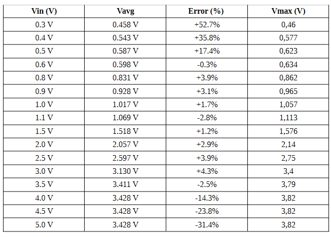
In this test, the input frequency was fixed at 500 kHz while the input voltage amplitude was varied in order to investigate the circuit behavior under different signal levels. According to the simulation results, the circuit was able to track the input signal with relatively low error within the approximate range of 0.6 V–3.5 V.
At low input voltage levels, the error rate increased due to diode effects and op-amp offset voltage. In particular, within the 0.3–0.5 V range, the diode forward voltage effect became more dominant, significantly reducing measurement accuracy.
At higher input voltages, the output approached saturation around 3.82 V due to op-amp output limitations and diode behavior. As a result, peak tracking accuracy decreased considerably for input levels above 4 V.
The component values used in these simulations are given below:
R3 = 10 kΩ, R4 = 1 kΩ, C2 = 10 nF and R5 = 2.2 kΩ.
4.1.4 Results and Limitations
Overall, the conventional peak detector circuit was able to provide satisfactory performance within certain frequency and input voltage ranges. However, simulation results showed that peak tracking performance depends not only on the circuit topology, but also strongly on op-amp dynamic characteristics, diode behavior, RC time constant, and the operating conditions of the input signal.
In addition, simulation results showed that even when a rail-to-rail op-amp was used, the output voltage could not fully reach the supply rails. This behavior is mainly caused by dynamic limitations of the op-amp output stage, load effects, and voltage losses occurring under high-frequency operating conditions. Therefore, op-amp output limitations should be carefully considered in peak detector design, and sufficient voltage margin should be maintained between the supply rails and the intended output level.
4.2 Improved Peak Detector Simulation
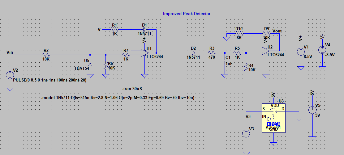
In this section, the improved peak detector circuit is analyzed. In the reference structure, a 10 MΩ resistor is used to discharge the hold capacitor. However, because this resistance value is quite large, the discharge time of the capacitor becomes excessively long, causing the previously stored peak information to remain for an extended period. Particularly under low-frequency or discontinuous input signal conditions, this behavior may introduce measurement uncertainty.
To reduce this effect, an ADG801 analog switch was added to provide controlled discharge of the hold capacitor. In this way, residual voltage from previous measurements was removed, ensuring that each measurement corresponded only to the current input signal. However, because the improved peak detector structure is more sensitive to high-speed transient behavior and sudden discharge currents, an additional series resistor was inserted between the capacitor and the discharge path. This structure reduces sudden discharge currents and improves output stability.
The R2 and R6 resistors at the input stage form a voltage divider that attenuates the input signal by approximately 50%. This structure protects the op-amp input and contributes to more controlled circuit operation. To compensate for this amplitude reduction, additional voltage gain was introduced at the non-inverting output amplifier using resistors R9 and R10. As a result, the output level was restored and the peak information could be transferred to subsequent measurement stages at a more suitable signal level. In the simulations, this gain value was adjusted according to different operating conditions and application requirements.
4.2.1 Improved Peak Detector Response Under Different Input Voltage Levels
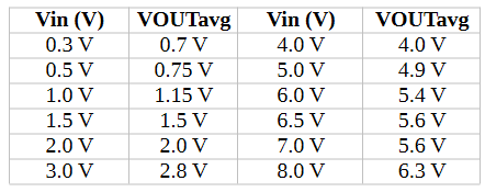
LTspice simulations performed at a 5 MHz input frequency showed that the circuit was sensitive to variations in input voltage amplitude. It was observed that measurement accuracy decreased particularly at very low and high amplitude levels. At low input levels, op-amp offset voltage, diode behavior, and charge injection effects became more dominant, while at higher input levels, op-amp dynamic limitations and transient response effects reduced output stability.
Simulation results showed that changes in input amplitude directly affected the peak tracking performance of the circuit, especially under short-duration pulse conditions.
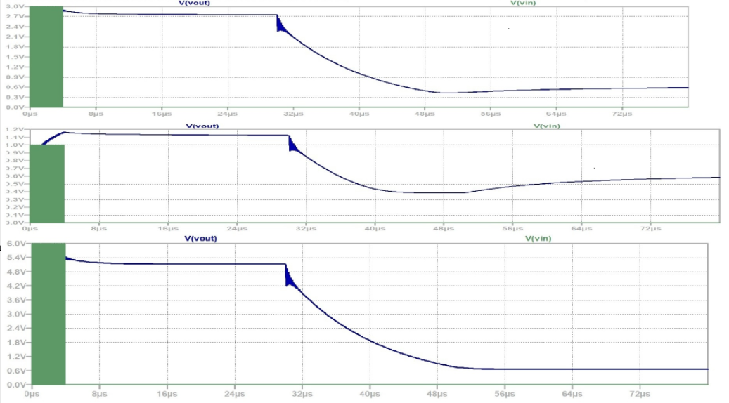
At a 5 kHz input frequency, the output behavior of the circuit appeared more stable compared to the 5 MHz operating condition. However, measurement errors caused by variations in the input voltage amplitude were not completely eliminated.
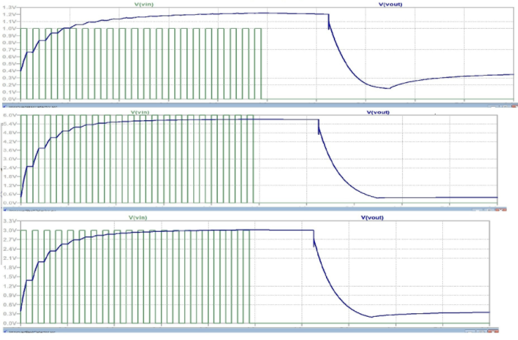
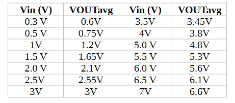
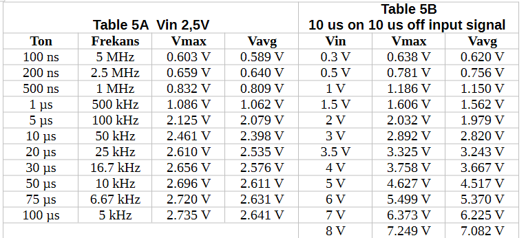
The presented simulations do not establish a consistent advantage for the modified topology. Because the operating points and gain settings are not identical across all runs, they also do not establish equal accuracy or a common usable frequency range. A controlled comparison with the same pulse shape, supply conditions, load, reset timing, and sampling instant is needed to quantify the difference.
Op-amp dynamics, charging time, diode behavior, and reset transients are plausible contributors to the observed errors. The plots alone do not isolate their individual contributions. Parameter sweeps and a corrected supply/model setup are needed before assigning a dominant cause.
4.3 What the Presented Simulations Show
| Simulation case | Reported observation | Interpretation limit |
|---|---|---|
| Conventional circuit, 2.5 V input | Best tracking reported around 500 kHz–1 MHz in the illustrated runs | Applies to those pulse and circuit settings; not a verified hardware bandwidth |
| Conventional circuit, 500 kHz | Relatively low error reported around 0.6–3.5 V; output approaches 3.82 V at higher input levels | No numerical error tolerance is established here |
| Modified circuit, 5 MHz | Output response varies with input amplitude | Does not by itself identify the dominant error source |
| Modified circuit, 5 kHz | More stable response than the illustrated 5 MHz case, with residual amplitude error | Does not establish superiority over the conventional circuit |
5. Conclusion
This LTspice study examines how charging time, op-amp dynamics, diode behavior, and hold-capacitor reset affect active peak detection. The examples show that adding circuit complexity does not automatically produce a more accurate peak estimate under the simulated conditions.
The next step is to resolve the supply and device-variant mismatch, then compare both circuits under a common set of conditions. Peak error should be evaluated at a defined sampling instant, with droop and reset settling assessed separately. Simulations should then be checked against bench measurements before assigning a hardware operating range.
For optical sensing, the useful design target is the required peak accuracy for a specified pulse amplitude, width, and repetition rate. Those requirements provide a clearer basis for choosing a topology than a general claim that one circuit is faster or more advanced.
References
[1] P. Horowitz and W. Hill, The Art of Electronics, 3rd ed., Cambridge University Press, 2015.
[2] The original study referred to an LTC6244 peak-detector application circuit without an application-note number or page reference. That attribution remains unverified; the circuit figures here should be treated as study schematics, not as verified manufacturer reference designs.
[3] Analog Devices, LTC6244 / LTC6244HV Datasheet, Rev. B, including supply ranges and absolute maximum ratings.
[4] S. Franco, Design with Operational Amplifiers and Analog Integrated Circuits, 4th ed., McGraw-Hill, 2014.