1. INTRODUCTION
This is Part 2 of the series. If you have not read it yet, you can start with Part 1 – Foundations.
When you step into the world of optical sensing, you are greeted by an infinite universe of colors and wavelengths. In the previous section, we embarked on a long journey through this universe, exploring how light behaves across the spectrum—from visible light to UV, and from infrared to NIR bands.
In this section, however, we are no longer carrying that entire map with us. We take only a single compass from our bag: the Infrared (IR) band.
And the journey begins with one fundamental question:
👉 “How does light turn into electricity?”
This question leads us to the two essential players of an optical system: the receiver (photodetectors) and the transmitter (LED and laser sources).
This week, I explain how the selection of photodetectors and transmitters determines the fate of an optical design.
If you’re ready — let’s begin.
2 – PHOTODETECTORS
Optical sensing systems are essentially an “art of extracting information from light.” The most critical component of the transmitter–receiver architecture is the photodetector.
In this section, we do not merely define the photodiode and the phototransistor — we also summarize all their parameters and their impact on system design.
2.1 Photodiode – General Definition
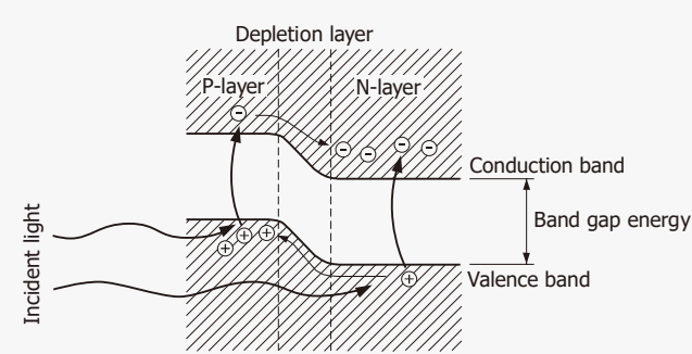
A photodiode is a semiconductor device that generates current by separating electron–hole pairs created by photons within the depletion region of a PN junction.
Low capacitance → very fast response High linearity → predictable signal
For this reason, it is the first choice in systems where speed is critical.
2.2 Phototransistor – General Definition
A phototransistor is a BJT transistor whose base region is made sensitive to light. Incident light generates a small base current, which is amplified by the β gain and converted into a collector current.
Result: Higher signal amplitude → easier detection However → slower response time
Compared to a photodiode, producing a signal that is 10–200 times larger makes it ideal for ON/OFF sensors; however, it can become a limiting factor in high-speed systems.
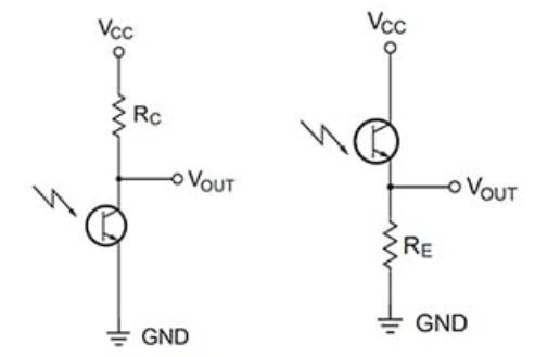
Source: DigiKey, adapted from Mechapedia / Northwestern University.
2.3 Photodetectors – Technical Analysis of Common and Distinct Parameters
Photodetectors (photodiodes and phototransistors) are semiconductor devices that convert light into an electrical signal. Although both sensors operate based on similar physical principles, the way their parameters affect circuit behavior and overall performance differs significantly.
Below, the parameters common to both detectors and their differing operating characteristics are summarized.
2.3.1 Common Parameters
(The same physical concept exists in both detectors; however, their behaviors differ.)
2.3.1.1 Radiant Sensitive Area (Effective Light-Sensitive Area)
Definition: The active surface area of the photodetector that collects light. The generated current is directly proportional to this area.
In photodiodes:
- The active area is generally larger.
- Larger area → collects more light.
- However, as the area increases, junction capacitance (Cj) increases → speed may decrease.
- In high-speed systems such as fiber optics and LiDAR, small-area photodiodes are typically preferred.
In phototransistors:
- The active area is smaller.
- Less light is collected; however, due to β gain, the collector current (IC) can be high.
- Smaller area → narrower field of view.
2.3.1.2 Shunt Resistance (RSH)
Definition: A parallel resistance representing leakage paths in the device, affecting noise performance.
In photodiodes:
- RSH is very high → low leakage → cleaner signal.
In phototransistors:
- Physically present, but it does not dominate circuit behavior.
- Noise is primarily determined by ICBO and ICEO leakage currents.
- Since leakage currents are amplified by β, RSH becomes practically insignificant.
2.3.1.3 Junction Capacitance (Cj)
Definition: The capacitance of the depletion region. It is one of the key parameters determining sensor speed.
In photodiodes:
- Cj is small → very fast response on the order of nanoseconds.
- Applying reverse bias further reduces Cj.
In phototransistors:
- Base–collector capacitance is large.
- Minority carrier storage is present.
- Result: slow response times in the microsecond to millisecond range.
2.3.1.4 Series Resistance (RS)
Definition: The internal series resistance, which forms part of the RC time constant.
In photodiodes:
- RS is low.
- Combined with low Cj, the system response is very fast.
In phototransistors:
- RS together with large capacitance further reduces speed.
2.3.1.5 Responsivity (A/W)
Definition: The generated current per watt of incident optical power.
In photodiodes:
- Linear and well-defined.
- Typical value for silicon photodiodes: ~0.4–0.6 A/W.
In phototransistors:
- Cannot be directly defined.
- Light first generates a small photocurrent → this current is then amplified by β.
- The response is non-linear, with a strong tendency toward saturation.
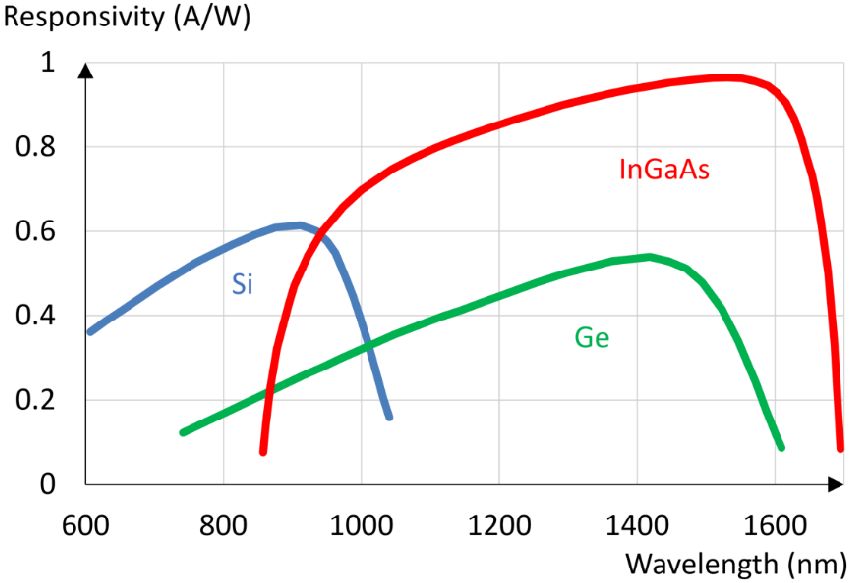
Source: Azadeh, Fiber Optics Engineering, Springer.
2.3.1.6 – Dark Current (Idark)
Definition: The leakage current that exists in the absence of light and serves as a source of shot noise.
In photodiodes:
- Low → high sensitivity.
In phototransistors:
- Much higher.
2.3.1.7 – Rise Time / Fall Time
Definition: The response time of the sensor to changes in incident light.
In photodiodes:
- Nanosecond range → very fast.
In phototransistors:
- Standard phototransistors: 10–50 µs.
- Darlington types: 1–10 ms → very slow.2.3.1.8 – Breakdown Voltage (Vbr)
Definition: The voltage at which uncontrolled conduction begins under reverse bias.
In photodiodes:
- Exceeding this voltage can cause damage (except for APDs).
In phototransistors:
- Based on a similar principle; however, it is less critical in practice since low bias voltages are typically used.
2.3.1.9 – Reverse Light Current (Iphoto)
Definition: The photocurrent generated when light strikes the photodetector while it is under reverse bias.
In photodiodes:
- Linear.
In phototransistors:
- The output current is much larger.
- However, controllability is lower.
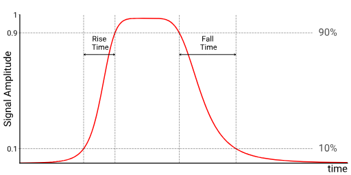
Source: Adapted from standard 10–90% photodetector timing definition.
2.3.1.8 – Breakdown Voltage (Vbr)
Definition: The voltage at which uncontrolled conduction begins under reverse bias.
In photodiodes:
- Exceeding this voltage can cause damage (except for APDs).
In phototransistors:
- Based on a similar principle; however, it is less critical in practice since low bias voltages are typically used.
2.3.1.9 – Reverse Light Current (Iphoto)
Definition: The photocurrent generated when light strikes the photodetector while it is under reverse bias.
In photodiodes:
- Linear.
In phototransistors:
- The output current is much larger.
- However, controllability is lower.
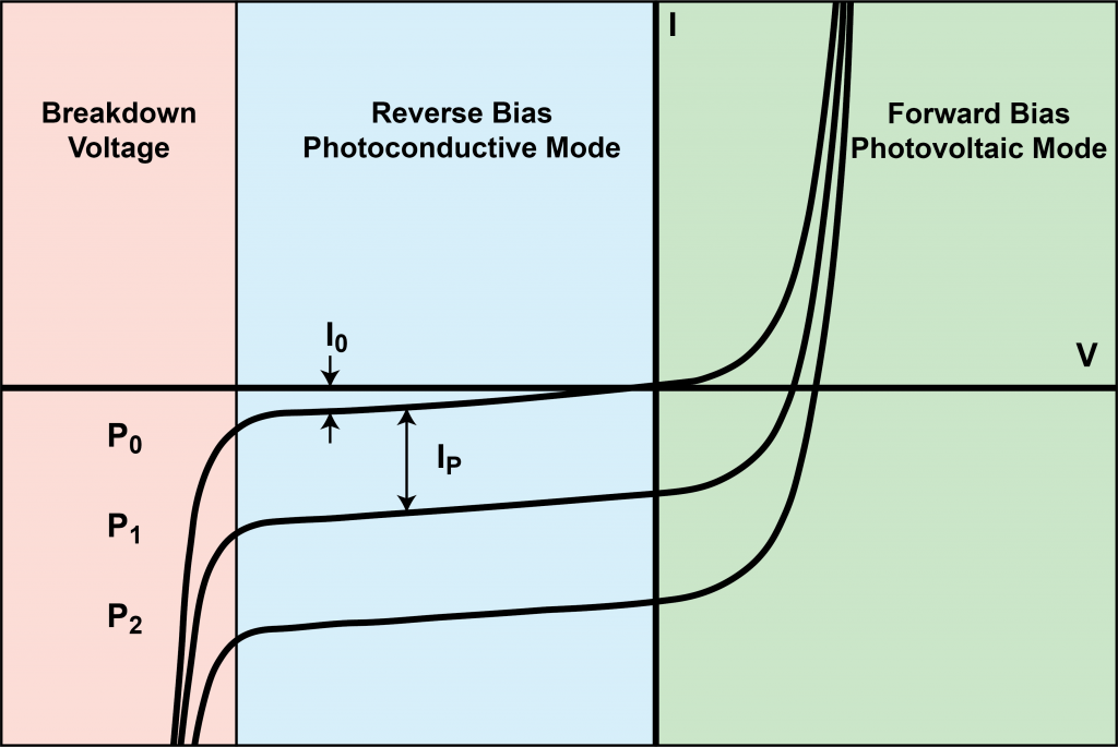
Source: University of Arizona, Photodetectors lecture notes.
2.3.1.10 – Temperature Coefficient
Definition: The coefficient that describes how device parameters vary with temperature.
In photodiodes:
- Voc, Isc, and noise are temperature-dependent.
In phototransistors:
- Both Iphoto and β are affected by temperature.
- Therefore, parameter drift is higher.
2.3.1.11 – Angular Sensitivity (Θ½)
Definition: The half-angle of the photodetector’s field of view. It is defined as the angle at which sensitivity drops to 50% when deviating from the optical axis. This angle represents the numerical definition of the Field of View (FOV).
In photodiodes:
- Wide field of view.
- More homogeneous response.
In phototransistors:
- Narrower field of view.
- More sensitive to angular misalignment.
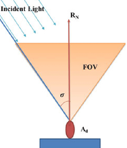
Source: Adapted from standard photodetector FOV geometry.
2.3.1.12 – Spectral Sensitivity (Range & Peak Sensitivity)
Definition: Indicates the wavelength range to which the sensor is responsive and the wavelength at which its sensitivity reaches a maximum.
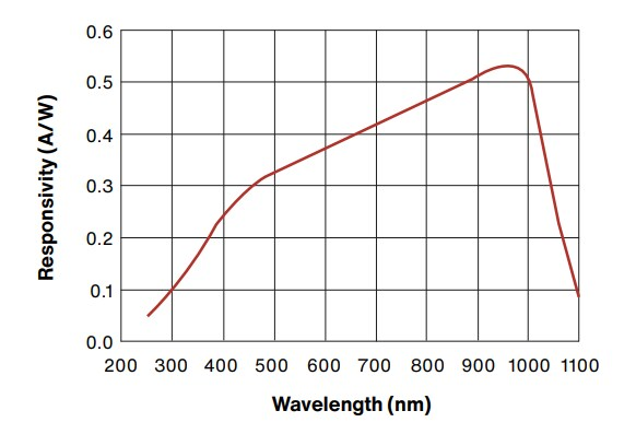
Source: Adapted from S. O. Kasap, Optoelectronics.
2.3.2 PARAMETERS UNIQUE TO PHOTODIODES
2.3.2.1 Forward Voltage (Vf)
- The forward conduction voltage.
- Relevant in photovoltaic mode.
2.3.2.2 Open-Circuit Voltage (Voc)
- The voltage generated under illumination in an open-circuit condition.
2.3.2.3 Short-Circuit Current (Isc)
- The short-circuit current generated under illumination.
- Used in photovoltaic measurements.
2.3.3 PARAMETERS UNIQUE TO PHOTOTRANSISTORS
2.3.3.1 Collector Current (IC)
- The main output current: IC = β × Iphoto
2.3.3.2 Transistor Gain (β)
- Determines how many times Iphoto is amplified.
2.3.3.3 Saturation Voltage (VCE(sat))
- Under excessive illumination, the transistor enters saturation.
- The output level becomes limited.
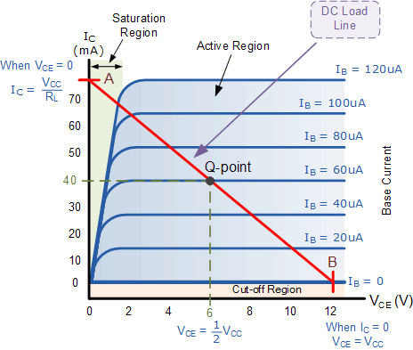
Source: IIT Bombay, EP215 Electronics Lab.
2.3.4 Photodiode – Phototransistor Comparison Table
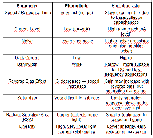
2.3.5 Photodiode or Phototransistor for Our Project? Let’s Make an Engineering Decision with Two Real Scenarios
In electronic design, we often encounter the following question: “Should I use a photodiode or a phototransistor in this project?”
When datasheets are reviewed individually, the answer is not always clear, because the correct component selection depends on the application.
In this section, we will seek an answer to this question not theoretically, but through two real project scenarios:
- Encoder design – speed measurement
- ON/OFF sensor / diffuse sensor – a system operating under ambient light
In both projects, we will use two very similar components from OSRAM:
- SFH 213 FA – Photodiode
- SFH 313 FA – Phototransistor
And we will try to give a clear answer to the question: “Under which conditions does the photodiode win, and under which conditions does the phototransistor win?”
First, we will examine the characteristics of both photodetectors in detail, and then quickly move on to the design scenarios.
2.3.5.1 Comparison of SFH 213 FA and SFH 313 FA
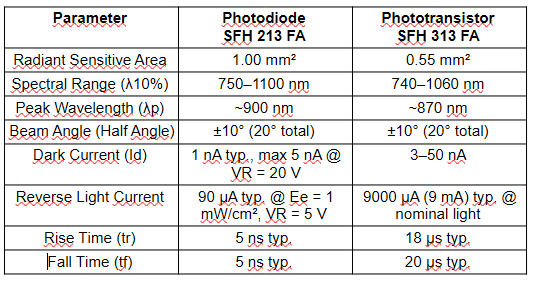
2.3.5.2 Circuits to Be Used
In our tests, we will use the following receiver circuits.
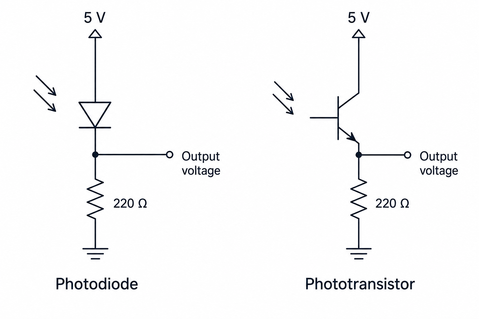
Source: Author’s illustration.
2.3.5.3 Theoretical Output Levels
SFH 313 FA – Phototransistor (R = 220 Ω) Ee = 0.5 mW/cm² → produces a collector current of 9 mA.
In this case, the output is: Vout = 9 mA × 220 Ω ≈ 2 V
SFH 213 FA – Photodiode Ee = 1 mW/cm² → 90 µA
For this photodiode current, let us examine two different load resistor scenarios:
- R = 220 Ω → Vout ≈ 90 µA × 220 Ω ≈ 20 mV
- R = 22 kΩ → Vout ≈ 90 µA × 22 kΩ ≈ 2 V
Note: In the photodiode circuit, to reach the same output voltage (~2 V) as the phototransistor, the load resistance must be increased by approximately 100×. The cost of this is a significant increase in the rise and fall times of the signal due to the larger RC time constant. Since we aim to design a fast photodiode circuit, we do not prefer this approach; instead, we assume that the photodiode output is taken quickly with a low resistance and then amplified to the 2 V level using an op-amp.
Project 1 – Encoder Design: Photodiode or Phototransistor?
Since we have not yet moved on to the transmitter section, at this stage we assume the use of an IR transmitter with a peak emission wavelength in the 850–900 nm range. Because the optical angles (half angles) of the photodiode and phototransistor are very similar, we ignore this effect for now.
In this project, the two main parameters we will compare are gain and speed.
To see how a simple optical encoder works, you can take a look at the following video: https://www.youtube.com/watch?v=_45VomiyUk0
Now that we understand the encoder principle, we can move on to the design.
On the receiver side, there are two different hardware configurations: a photodiode-based receiver and a phototransistor-based receiver. In the following sections, we will examine all details both optically and electrically; at this stage, we are evaluating only the photodetector outputs.
TEST-1
- Encoder disk: 200 slots
- Motor speed: 300 rpm
- 300 rpm = 5 rps
- Pulse frequency: 200 × 5 = 1 kHz
- Period: T = 1 / 1 kHz = 1000 µs
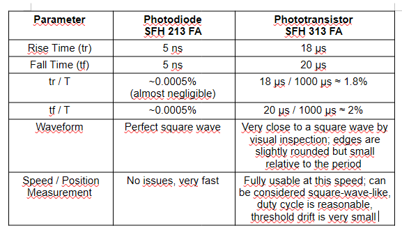
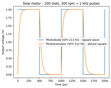
Source: Author’s simulation.
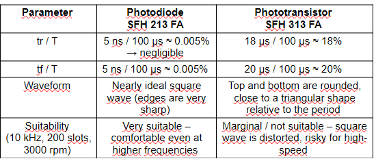
TEST-2
- Encoder disk: 200 slots (same)
- Motor speed: 3000 rpm (10× faster)
- 3000 rpm = 50 rps
- Pulse frequency: 200 × 50 = 10 kHz
- Period: T = 1 / 10 kHz = 100 µs
Conclusion: Although the SFH 313 FA may appear advantageous at the beginning of the design, we observe that it performs well only at low speeds. As the speed increases, the slow response time of the phototransistor distorts the waveform and poses a serious risk for high-frequency encoder applications.
Design-2: Optical ON/OFF Switch – Photodiode & Phototransistor
At first glance, an optical barrier switch appears quite simple. Here, we are referring to a detector similar to the one shown in the following video:
🔗 https://www.youtube.com/watch?v=l1rjErRvbgw&t=265s
However, behind this simple structure lies a critical design reality—especially under conditions where ambient light continuously changes: the choice of receiver causes the entire system to behave differently.
In this section, we build a “realistic” optical barrier circuit and compare two different receivers under the same optical transmitter. Our goal is to observe how these two detectors respond under real-world conditions such as sunlight, IR heaters, and artificial lighting.
1. Experimental Setup – Placing Two Different Receivers in the Same Scene
We assume that a 10 kHz signal is transmitted from the emitter.
3. Test Objective – Different Receivers Under the Same Light
In the experiment, we observed how the sensors behave under:
- Strong transmitter light
- Weak light
- Shadow
- Direct sunlight
- Presence of ambient reflections
4. Measurements – Outputs Under a 10 kHz IR Signal
Phototransistor-based circuit:
- Despite the high-amplitude transmitter signal, intense daylight caused an approximately 1.8 V DC base level at the output.
- Since the transistor saturated around the 2 V level, the 10 kHz carrier signal was clipped at the upper level; the square waveform was severely distorted.
- Because the rise/fall times (≈ 18–20 µs) correspond to roughly 20% of the 10 kHz signal period, the edges became rounded and the signal lost its square-wave character.
- The noise level was noticeably higher compared to the photodiode-based circuit.
Photodiode-based circuit:
- Due to the much lower gain on the photodiode side, no saturation problem occurred under ambient light.
- The output level remained on the order of tens of millivolts; this signal can be safely amplified later using op-amp circuits, while the DC base component can be separated with high-pass filters.
- The 10 kHz signal preserved its square-wave form; the observed distortion was negligible.
- Both noise and DC offset were lower in the photodiode-based circuit compared to the phototransistor.
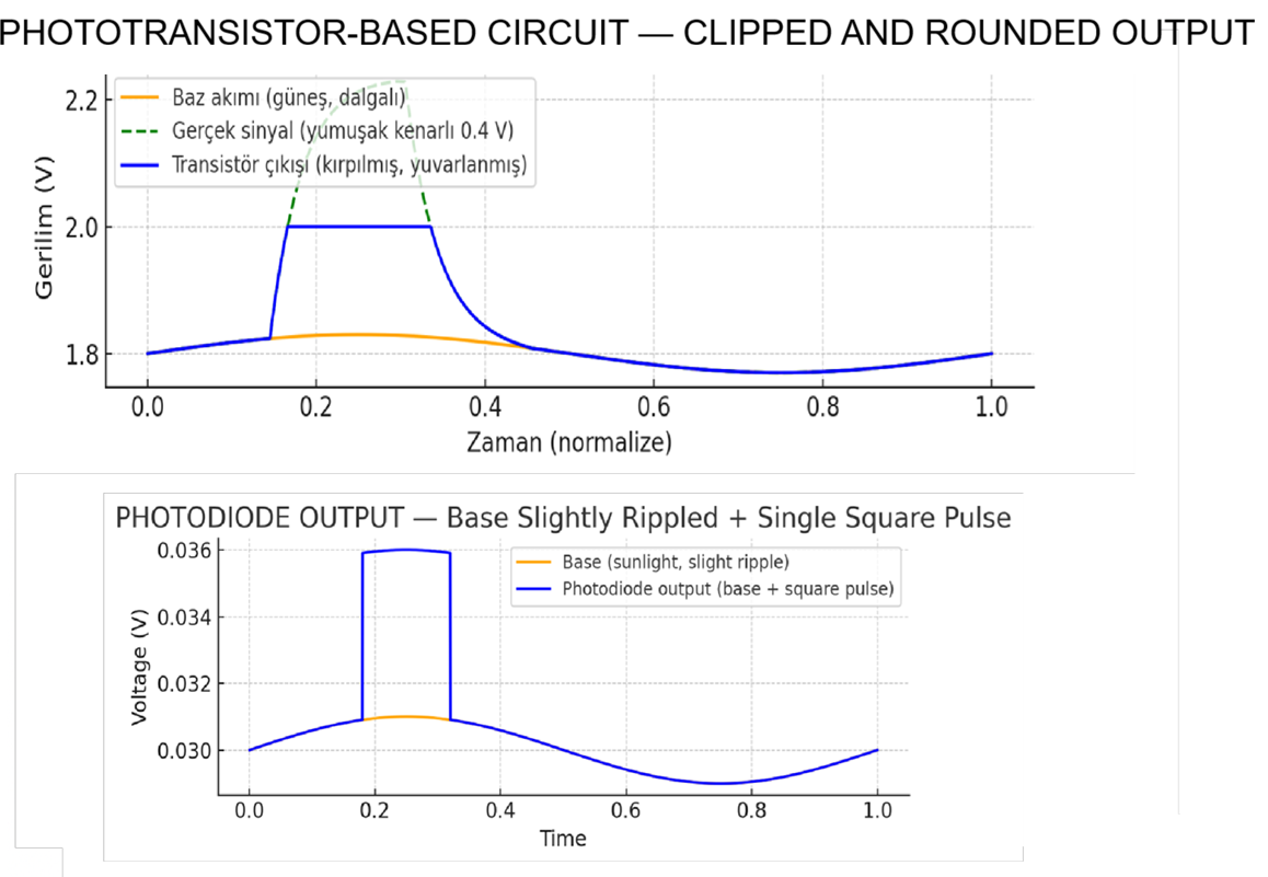
Source: Author’s simulation.
2.3.6 Photodetectors – Summary
Photodiodes and phototransistors are semiconductor sensors that convert optical signals into electrical current; however, their speed, gain, and noise performance differ significantly.
Thanks to its low junction capacitance, the photodiode offers rise/fall times on the order of nanoseconds and is ideal for encoders, modulated IR sensing, and high-speed optical communication systems that require wide bandwidth.
The phototransistor, on the other hand, amplifies the photocurrent by the β factor to produce an output at the milliampere level; however, due to carrier storage, it exhibits response times in the microsecond to millisecond range.
Under ambient light conditions, the phototransistor easily generates DC offset and saturation, whereas the photodiode provides a more linear, more predictable, and cleaner signal in terms of noise.
Therefore, the selection criterion is clear: if bandwidth and speed are critical, the photodiode is preferred; if high signal amplitude and simple threshold detection are required, the phototransistor is the better choice.
3. Transmitter Source Type Selection
3.1 Introduction
The word “laser” still evokes cinematic scenes for many people: the beams slicing people into cubes in the movie Cube, the sharp line of a lightsaber, or Catherine Zeta-Jones gliding through a web of laser beams in a laser-protected museum in Entrapment…
These scenes portray the laser almost like an invisible knife. In reality, engineering does not work that way.
A laser is light produced with a very narrow divergence, phase coherence, and high directionality. An LED, on the other hand, is a more diffuse, wide-angle, homogeneous light source that is, in most applications, far more controllable, economical, and safe.
For the designer, the critical question is: “Should I use an LED or a laser as the transmitter?”
This decision directly determines the system geometry, range, optical alignment tolerances, safety class, and receiver architecture.
This section summarizes all the physical and engineering background required to make the correct transmitter selection.
3.2 Transmitter Source Type Selection – LED or Laser?
LEDs and lasers are fundamentally different types of optical sources in terms of how they generate light and how that light propagates.
The key to understanding this difference correctly is knowing how light spreads in space and how it is shaped.
The following section will clearly and concisely present the physical and mathematical foundations of the distinction between LEDs and lasers, and will also explain—based on engineering reasoning—why a designer must choose an LED in some applications and a laser in others.
3.3 LED and Laser Transmitters – Parameters
3.3.1 Common Parameters
3.3.1.1 Wavelength (λ)
Indicates the spectral region in which the source emits light.
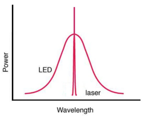
Source: Adapted from standard LED–laser spectral characteristics.
LED:
- Emits a broad spectrum (wide bandwidth).
- An 850 nm LED radiates light in the 810–900 nm range.
- Matching with a photodetector can be more challenging; however, cost is low.
Laser:
- Emits light in a very narrow spectrum (single line).
- Easier matching with the detector → higher efficiency.
What is it useful for?
- If a filtered receiver is used → the laser is more stable.
- In applications such as infrared barrier sensors → an LED is sufficient.
3.3.1.2 Modulation Frequency
Indicates how fast the source can be switched on and off.
LED:
- Can be modulated up to the MHz range.
- More than sufficient for ON/OFF and 10–100 kHz IR applications.
Laser:
- Can be modulated at very high speeds (GHz range).
What is it useful for?
- High-speed communication → laser.
- Simple IR sensor applications → LED.
3.3.1.3 Beam Angle (Half Angle – Beam Divergence)
Shows how much the light spreads in space.
LED:
- Typically 20°–60°.
- Illuminates a wide area → easy alignment.
Laser:
- Has a beam divergence on the order of milliradians.
- Provides long range and a sharp beam.
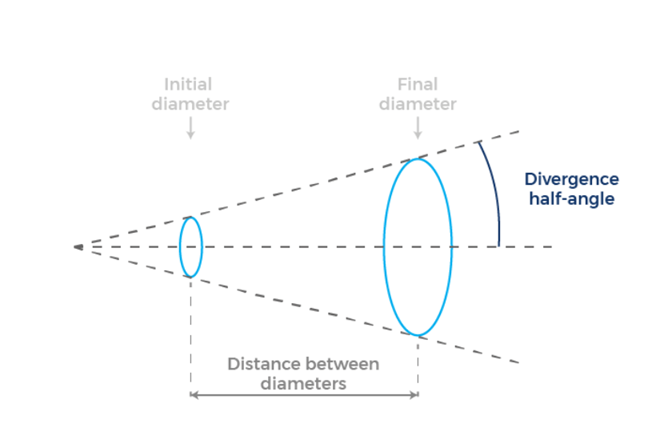
Source: Gentec-EO.
3.3.1.4 Radiant Intensity / Optical Power
LED:
- Expressed as Iv (mW/sr).
- Since the light spreads over a wide area, the intensity is low.
Laser:
- Produces optical power at the mW level.
- However, it is focused into a very narrow area.
- Provides high intensity even at long distances.
What is it useful for?
- If you want a signal that does not get lost under sunlight → laser.
- For short-range sensor applications → LED is sufficient.
3.3.2 PARAMETERS UNIQUE TO LEDs
3.3.2.1 Radiant Intensity (Iₑ)
Indicates how strongly the LED emits light in a specific direction.
What is it useful for?
- Between two LEDs with the same optical power, the one with a higher Iₑ value carries light farther.
3.3.2.2 Total Radiant Flux (Φₑ)
The total optical power produced by the LED (mW).
What does it mean?
- Larger Φₑ → more powerful LED.
- However, due to wide-angle emission, long range is not always guaranteed.
3.3.2.3 Forward Voltage (VF)
The forward voltage applied to the LED.
Impact on design:
- Determines the supply level of the driver circuit.
- When selecting an LED, VF and current rating must always be evaluated together.
3.3.2.4 Reverse Voltage (VR)
The maximum voltage the LED can withstand when reverse-biased.
What is it useful for?
- Determines whether protection diodes are required.
3.3.2.5 Permissible Pulse Handling Capability
The LED’s ability to withstand short-duration high currents.
Impact on design:
- A critical parameter in modulated (pulse-driven) IR LED drivers.
- Currents as high as 1 A may be applied for short durations — provided the correct duty cycle is used.
3.3.3 PARAMETERS UNIQUE TO LASERS
3.3.3.1 Beam Quality (M²)
Indicates how closely the laser beam approximates an ideal Gaussian beam.
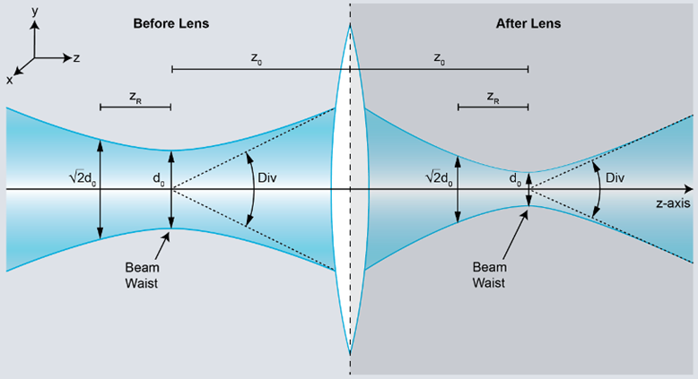
Source: Gentec-EO, Beamage-M² User Manual.
What is a Gaussian Beam?
A Gaussian beam is a transverse intensity profile of laser light in which:
- The intensity is highest at the center,
- It decreases smoothly toward the edges,
- It spreads very little over long distances,
- It is mathematically described by a Gaussian distribution.
What is the main difference compared to an LED?
- LED → Light spreads in a conical, non-uniform, wide-angle manner.
- Laser → Light has a Gaussian profile and does not diverge rapidly.
3.3.3.2 Coherence (Phase Coherence)
Indicates how orderly the phase of the light is.
Impact on design:
- Provides a stable beam over very long distances.
- Increases immunity to interference and noise.
3.4 Transmitter – Summary
By the end of this section, we can state the following very clearly:
LED → senses volume; Laser → senses a point
When designing an optical system, the first question you should always ask yourself is: “Am I measuring only a single point, or do I need to see its surroundings as well?”
Because the chosen source directly determines the geometry of the system.
An LED spreads over a wide angle, fills an area, and senses volume; a laser concentrates its energy into a single point, behaves like a line, and sees only that point.
If the light beams protecting the museum in the movie Entrapment had been LEDs instead of lasers, Catherine Zeta-Jones would not have been able to gracefully slip through the beams. An LED fills the entire area and leaves no escape gaps.
That is why the decision inevitably becomes:
- If you are scanning a volume, a wide region, or a surface → LED
- If you are measuring a single line, a small target, or a long distance → Laser
4 – Final Product Selection: How to Determine the Right Receiver & Transmitter
When designing an optical system, everything starts with a single question: “What am I sensing?”
The answer to this question automatically defines the selection order:
1) Wavelength First, the operating wavelength is selected. The peak wavelength of the transmitter and the peak sensitivity of the receiver must match.
2) Transmitter type (LED / Laser)
- LED → Wide angle, volumetric sensing, short to medium range
- Laser → Narrow angle, point sensing, long range
Question: Am I seeing a volume, or a single point?
3) Receiver type (Photodiode / Phototransistor)
- Photodiode → Speed and bandwidth
- Phototransistor → High signal level, low speed
Question: Is speed more important, or signal amplitude?
4) Optical angle and sensing area Will I see a wide area, or track a narrow line? Range and alignment tolerance are determined here.
5) Power and flux analysis “What is the minimum amount of light that must reach the receiver?” The answer determines the transmitter power and the expected photocurrent at the receiver.
6) Speed requirement Modulation frequency, rise/fall time, and bandwidth finalize the decision.
5 – Closing
In this section, we have seen how the correct selection of receiver and transmitter determines the fate of an optical system.
In the next section, we will no longer be designers who merely “sense” light—we will become designers who shape light.
Continue with Part 3A – Optical Elements: Lenses.
References
[1] Hamamatsu Photonics, Photodiodes Exposed: Unlocking the Characteristics of These Crucial Sensors, 2024.
[2] DigiKey, How to Use Photodiodes and Phototransistors Most Effectively.
[3] M. Azadeh, Fiber Optics Engineering, Springer.
[4] RSC, Best Practices in the Measurement of Photodetectors, 2022.
[5] S. O. Kasap, Optoelectronics and Photonics: Principles and Practices.
[6] IIT Bombay, EP215 Electronics Lab – BJT Characteristics and Load Line.
[7] Gentec-EO, Laser Beam Divergence and Diameter.
[8] Gentec-EO, Beamage-M² User Manual.