1. Introduction
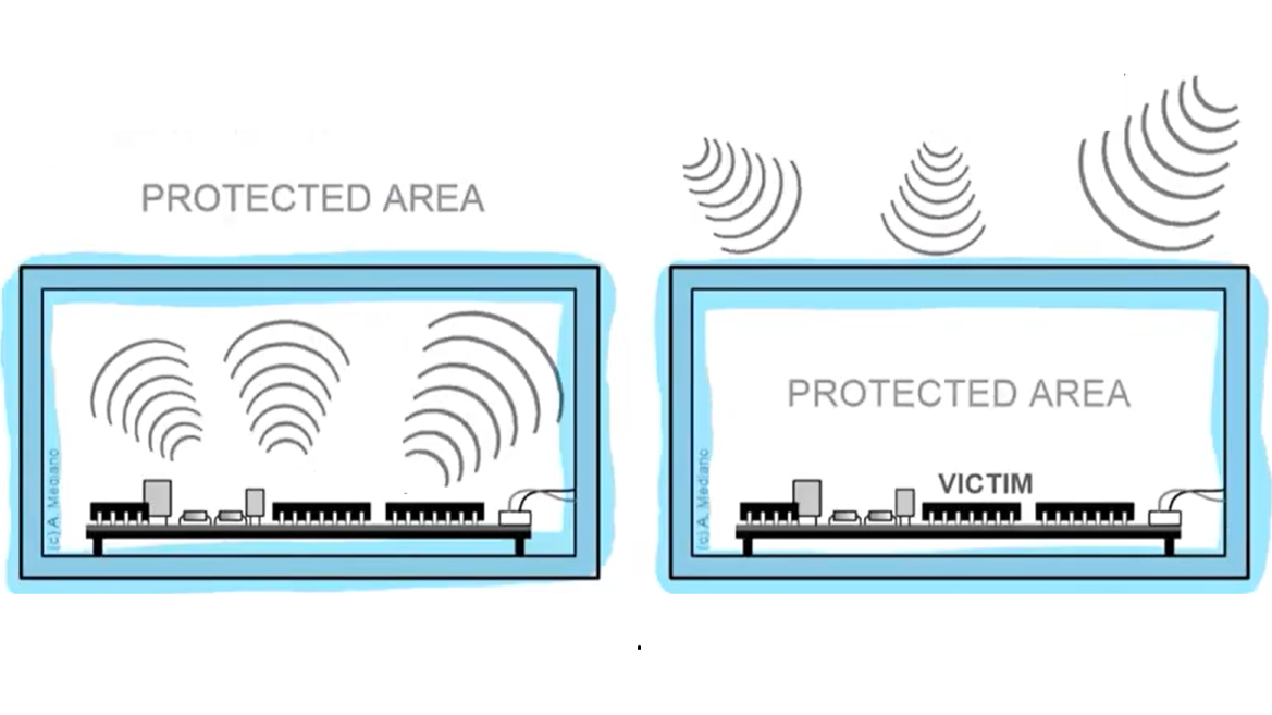
In mixed-signal PCB design, the coexistence of analog and digital circuits on the same board presents significant challenges related to electromagnetic interference (EMI). Analog circuits typically operate with low-level signals and are therefore highly sensitive to noise, while digital circuits generate fast switching currents that can easily couple into nearby sensitive analog sections.
Traditional design practices have long recommended separating analog and digital ground planes and placing decoupling capacitors of different values in parallel to mitigate these interactions.
However, modern EMC and signal integrity literature has begun to re-evaluate these traditional practices. In high-speed systems, discontinuities in the reference plane may disturb the natural return current path and increase electromagnetic emissions.
Despite these findings, some semiconductor manufacturers’ reference designs still include implementations that do not fully align with modern EMC guidelines. This discrepancy raises important questions about the relationship between theoretical recommendations and practical engineering implementations in mixed-signal PCB design.
2. Traditional Approaches: Star Ground and Split Ground Planes
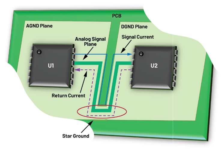
In early mixed-signal PCB design practices, star grounding and split ground plane techniques were widely used to reduce interference between analog and digital circuits. In this approach, the ground references of analog and digital circuits are physically separated and typically connected at a single point.
The primary goal of this method is to prevent digital switching currents from flowing through the reference path of analog circuits.
Henry W. Ott notes in his work on EMC design that star grounding can be useful for controlling noise currents, particularly in low-frequency systems. In this configuration, the return currents of analog and digital circuits follow separate paths and meet only at a single reference point.
3. Split Ground Plane Issues, Antenna Effect, and Return Current Behavior
The separation of analog and digital ground planes has been widely used in mixed-signal PCB design for many years. However, modern EMC and signal integrity literature has begun to re-evaluate these traditional practices. In high-speed systems, discontinuities in the reference plane may disturb the natural return current path and increase electromagnetic emissions.
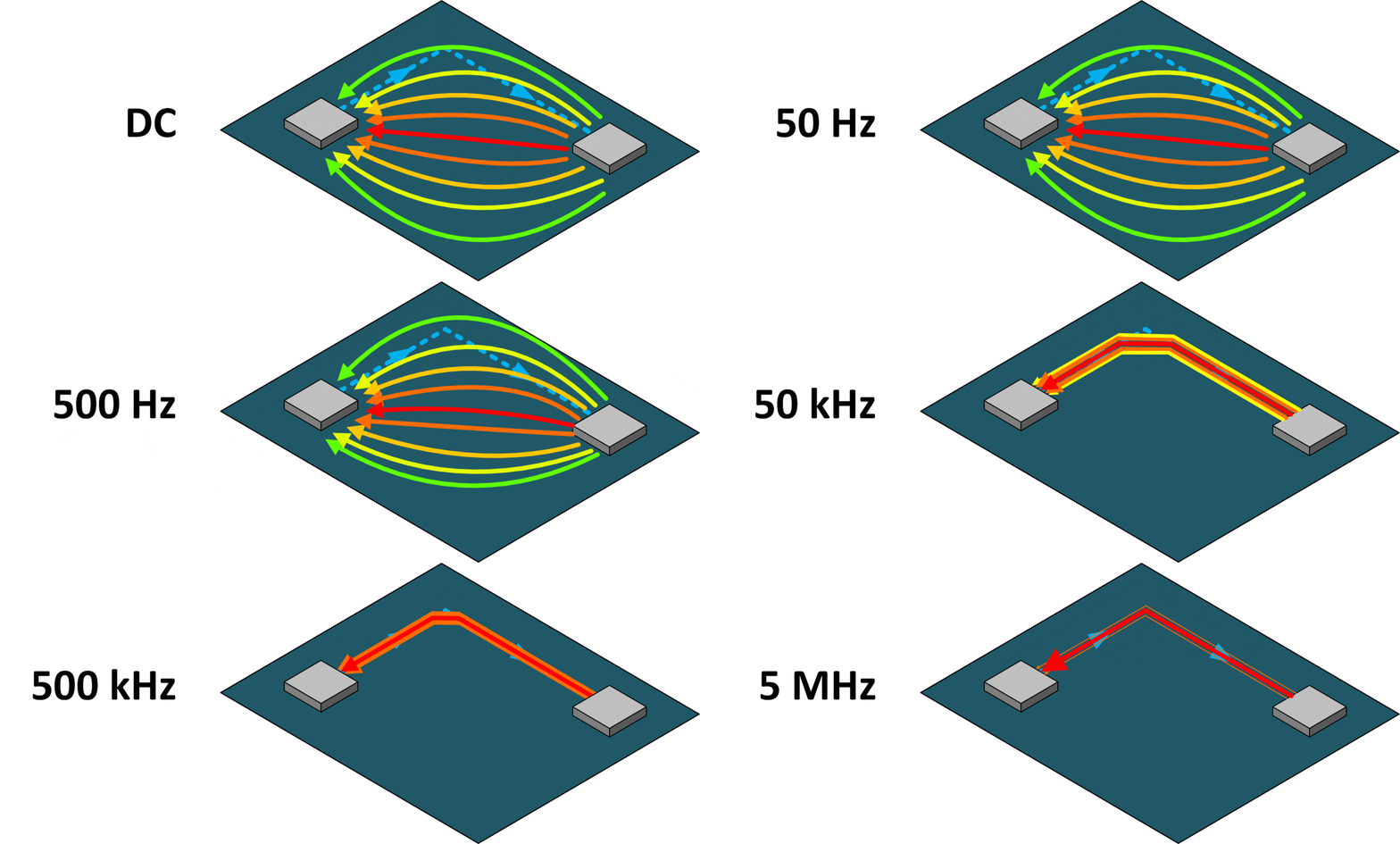
In a microstrip transmission line, the return current does not distribute uniformly across the reference plane. Instead, most of the current flows close to the signal trace. Measurements presented by Henry W. Ott quantitatively demonstrate this distribution.
In the table below, the parameter h represents the vertical distance between the signal trace and the reference ground plane, which corresponds to the dielectric thickness in the PCB stack-up. The parameter x represents the horizontal distance from the center of the trace. Therefore, the x/h ratio represents the horizontal distance normalized by the trace height.
For example, x/h = 3 corresponds to a horizontal distance equal to three times the vertical distance between the trace and the reference plane.
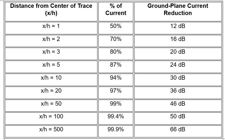
As shown in the table, the majority of the return current is concentrated very close to the signal trace. Approximately 80% of the current flows within 3h, and 94% within 10h.
These observations form the basis of the commonly cited 10h rule. According to this rule, discontinuities within approximately 10h of the signal trace in the reference plane may disrupt the natural return current path.
When the return current is forced to follow a longer path, the current loop area increases. A larger loop area results in stronger electromagnetic radiation. Therefore, discontinuities in the reference plane can behave like a loop antenna on the PCB, increasing electromagnetic emissions.
4. Layout Partitioning Instead of Return Reference Plane Separation
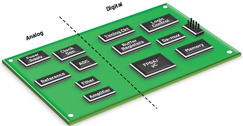
In modern mixed-signal PCB design, reducing interference is often achieved by layout partitioning rather than physically splitting the reference plane.
Since high-frequency return currents tend to flow directly beneath the signal trace in the reference plane, separating analog and digital circuit blocks physically on the PCB is often sufficient to reduce interference.
Typical layout guidelines include:
• Physically separating analog and digital circuit blocks on the PCB
• Keeping clock and high-speed digital signals within the digital region
• Routing sensitive analog signals away from digital traces
• Using a continuous ground plane
This approach preserves the natural return current path and reduces the interaction between analog circuits and digital switching noise
5. Parallel Use of Decoupling Capacitors and the Anti-Resonance Problem
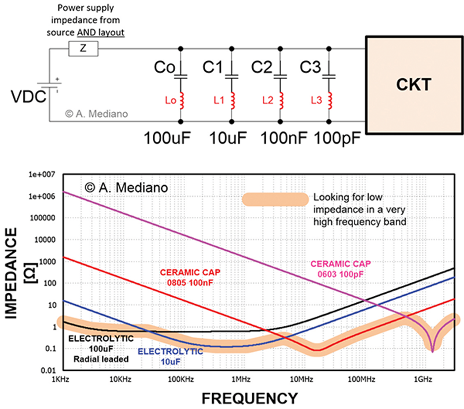
The use of decoupling capacitors with different values in parallel on power supply lines has long been recommended as a common design approach. The purpose of this method is to maintain low impedance across a wide frequency range in the power distribution network.
However, real capacitors are not ideal components. Each capacitor has an equivalent series resistance (ESR) and equivalent series inductance (ESL). Therefore, the frequency response of real capacitors differs from that of an ideal capacitor.
Although connecting capacitors of different values in parallel theoretically appears to provide low impedance across a wide frequency range, in practice the RLC behavior of capacitors may lead to anti-resonance. In such cases, the impedance of the power distribution network may increase at certain frequencies, reducing the effectiveness of decoupling [5].
For this reason, modern power distribution network design must consider not only capacitor values but also several additional parameters, including:
• capacitor placement
• connection inductance
• current loop area
These parameters play a critical role in determining the overall performance of the power distribution network.
6. Discussion
Reference designs are often used by engineers as a starting point when developing a new circuit. As a result, schematics and evaluation board layouts provided in datasheets can strongly influence design decisions.
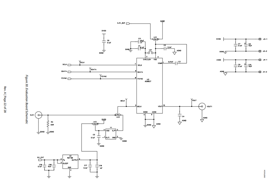
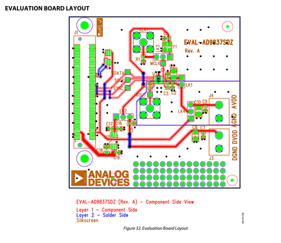
When the AD9837 evaluation board schematic and PCB layout are examined, it can be observed that the analog and digital ground regions are separated and connected at a single point using a star topology [6].
However, mixed-signal PCB design guidelines published by Analog Devices state that separating analog and digital grounds is not always necessary. In many cases, the use of a continuous ground plane combined with layout-level separation of analog and digital circuit blocks is recommended [1].
Despite this recommendation, the AD9837 evaluation board design still employs a star-connected separation of analog and digital ground regions, and different values of decoupling capacitors are used on the power supply lines.
Therefore, reference designs should not be interpreted as strict design rules that must be directly replicated. Instead, they should be considered example implementations developed under specific design constraints.
7. Conclusion
In mixed-signal PCB design, the coexistence of analog and digital circuits requires careful design decisions in order to control electromagnetic interference. Modern EMC and signal integrity literature generally recommends the use of a continuous reference plane and careful modeling of the power distribution network. Within this framework, it is often argued that separating analog and digital grounds is not always necessary and that the parallel use of decoupling capacitors with different values may introduce anti-resonance problems.
Nevertheless, some semiconductor manufacturers’ reference designs still employ analog and digital ground separation and the use of decoupling capacitors with different values. This discrepancy between the principles suggested in the literature and the practices observed in reference designs may create uncertainty for engineers designing mixed-signal systems.
This raises an important question: Do these reference designs still rely on valid engineering considerations, or should these traditional practices in mixed-signal PCB design be reconsidered?
References
[1] Analog Devices, What Are the Basic Guidelines for Layout Design of Mixed-Signal PCBs?, Analog Dialogue.
[2] Henry W. Ott, Electromagnetic Compatibility Engineering, Wiley.
[3] Howard Johnson, Martin Graham, High-Speed Digital Design: A Handbook of Black Magic. [4] Eric Bogatin, Signal and Power Integrity – Simplified.
[5] In Compliance Magazine, Using Capacitors in Parallel: Dangerous?
[6] Analog Devices, AD9837 Data Sheet.