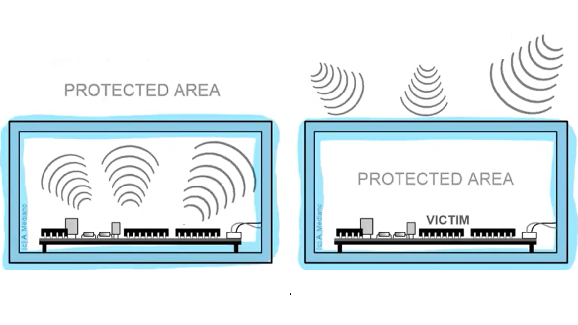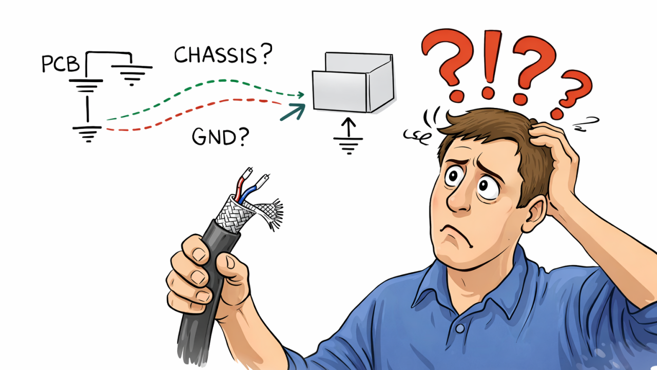
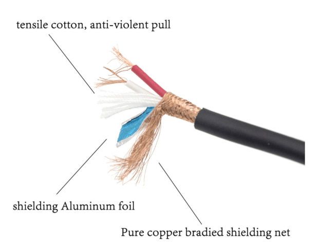
Figure attribution: The three connection diagrams in this article are author-generated illustrations based on standard EMC grounding principles. The enclosure, smartphone shielding, and cable-construction images are reproduced or adapted from the external sources identified in their captions.
1. WHAT IS A CABLE SHIELD — AND WHAT IS IT NOT?
In shielded cables, the conductors are surrounded by a braided and/or foil layer. This layer:
- Does not carry signal current
- Does not eliminate noise
- Provides a controlled return path for common-mode currents
When terminated incorrectly, however, the shield may:
- Act as an antenna
- Aggravate EMI and ESD problems
The issue is not the existence of the shield itself, but the way it is connected.
2. Why Is the Shield Connected to the Metal Chassis?
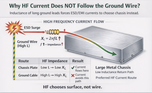
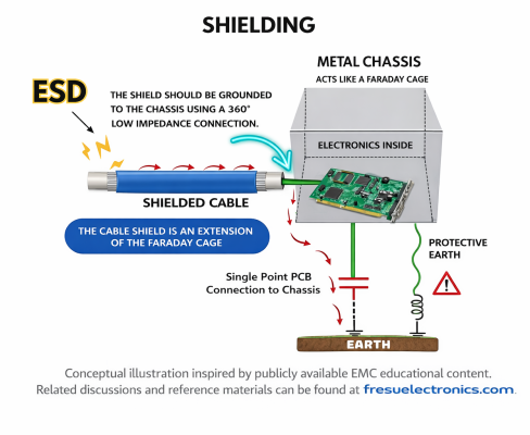
High-frequency EMI and ESD currents do not flow through signal ground (GND); they flow over large, low-impedance conductive surfaces. For this reason:
The cable shield is connected directly to the chassis.
Protective Earth (PE) serves as a safety reference, while PCB GND is a signal reference.
Neither is intended to carry high-frequency interference currents.
3. Why Does the Current Follow the Chassis Instead of PE?
Although the PE conductor may appear as nearly zero ohms at DC, it behaves as an inductive element at high frequencies.
This is because grounding conductors are inherently inductive.
As a rule of thumb:
- 10 cm of wire corresponds to approximately 5–20 nH
- 1 nH presents about 6 Ω at 1 GHz
- 20 nH corresponds to roughly 120 Ω
As a result, high-frequency currents avoid the PE path and instead flow along the chassis.
The chassis, with its large surface area, provides a much lower impedance path at high frequencies.
4. Why Is a PCB–Chassis Connection Mandatory?
If the PCB is not referenced to the chassis, an ESD event causes the following situation:
- The enclosure potential rises abruptly
- The PCB remains at its original potential
- Energy couples capacitively into the PCB
The solution is straightforward:
The PCB ground must be referenced to the chassis at a single, wide connection point.
The objective is not to force current into the PCB, but to allow the PCB potential to rise together with the chassis.
5. The Single-Point Rule
A single-point connection means that PCB GND is bonded to the chassis through only one physical contact point.
If multiple connections are made:
- Ground loops are formed
- High-frequency currents circulate
- Antenna-like behavior is created
6. Where Should the Single Point Be Located?
The connection point should be:
- Close to the cable entry point
- At the shield termination location
- As short as possible between PCB and chassis
The shorter and wider the connection, the better its high-frequency performance.
7. What Is the Shield Connected to at the Other End?
At the opposite end of the cable, the shields are bonded together and tied to a common potential via PE.
In this way, EMI currents are confined to the chassis path and return without being coupled into the signal ground.
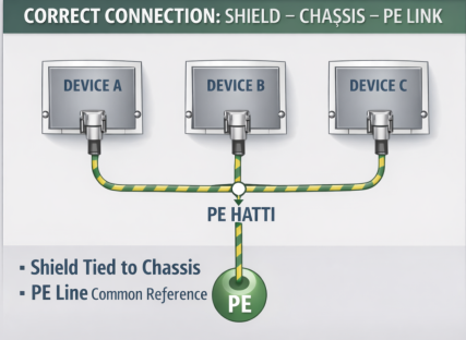
The Golden Rule
As illustrated, the cable shield is terminated at the connector entry by being pressed directly onto the chassis with a 360-degree circumferential contact. The PCB ground, on the other hand, is connected to the chassis at only a single point, using the shortest and widest possible connection—and this point should be located as close as possible to the cable entry.
The opposite end of the shield is brought to a common potential via the PE conductor. The role of PE here is not to “carry” the ESD current directly to earth; rather, PE serves purely as a reference.
Regardless of where a high-frequency ESD pulse originates, all conductive surfaces tend toward the same potential. Because the chassis presents a much lower impedance than thin conductors, the current spreads primarily over the chassis surface, and the energy is dissipated to earth through the capacitive coupling between the chassis and ground
8. Shield Termination in Plastic Enclosures
One important advantage of plastic enclosures is that, unlike metal chassis, they do not directly trigger ESD events. However, plastic housings are also unable to guide ESD energy to earth in the way a metal enclosure can.
When an ESD pulse strikes a plastic enclosure, the charge spreads over the surface, but because plastic is non-conductive, the current cannot find a defined discharge path. As a result, the energy couples into the PCB through electric-field effects and high dv/dt, or enters the circuit via electromagnetic coupling.
In a plastic enclosure, the core problem can be summarized as follows:
ESD enters the system but cannot find a return path → the energy is discharged through the circuitry.
This often leads to issues such as resets, lock-ups, SPI/I²C communication errors, and unintended GPIO triggering.
Design Objective
The primary goals are:
- To create a defined discharge path for ESD (hardware first)
- To design robust circuitry and software capable of absorbing the remaining disturbance
Mitigation Methods (Best to Weakest)
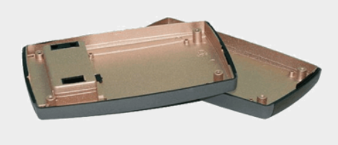
1) Adding a Metal Plate or Shield (BEST OPTION)
A conductive metal surface is placed on the inner wall of the plastic enclosure or beneath the PCB. This surface increases the parasitic capacitance to earth, providing a preferred path for ESD energy.
Design rules:
- The metal plate should be larger than the PCB
- TVS devices, filters, and ground references should be connected to this plate rather than directly to the PCB
- The connection between the plate and the PCB should be short and low-impedance
Result: ESD energy is discharged through the plate before entering the circuitry, significantly improving system robustness.
2) Connecting to the Return Ground Plane (MEDIUM LEVEL)
If no metal plate is available, the cable shield, TVS devices, and filters are connected directly to the PCB GND return plane. In this case, the current flows through the circuit, but along a controlled path, which reduces the potential damage.
Key points to consider:
- Filters must be placed as close as possible to the input connector
- Loop area must be minimized
- The software must be robust (watchdog enabled and reset protection implemented)
Result: Some level of protection is achieved, but it is not complete. ESD energy can still circulate within the circuit.
3) Direct Connection to the PCB (WEAK)
All ESD current circulates on the PCB, spreading over the ground plane and potentially disturbing sensitive signals. In this approach, the issue is not eliminated—its impact is only reduced.
Additional countermeasures required:
- RC filtering and TVS protection on reset and interrupt lines
- An EMI-robust PCB layout
- Firmware designed to handle crash and recovery scenarios
Result: The system may function, but passing compliance or immunity testing becomes difficult.
Summary
In plastic enclosures, ESD cannot be completely prevented. The design objective is to provide the energy with an escape path (metal plate or return plane) and to absorb the remaining disturbance using filtering and robust software.
9. ESD Protection in Mobile Devices (Phones and Tablets)
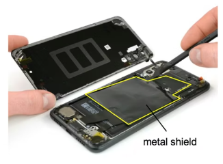
In mobile devices, there is no metal chassis or earth reference. ESD is therefore attenuated by distributing the energy across the device surfaces. The goal is not to dump the current to ground, but to spread the energy density and absorb it without damaging the circuitry.
Key methods:
- Adding internal metal foil or conductive surfaces → ESD energy is distributed over a wide area
- Placing TVS devices at entry points such as USB, buttons, and touch interfaces → The surge is blocked before entering the PCB
- Using a thin conductive layer (ITO or mesh) beneath the display → Surface charge is spread across the panel
- Implementing a GND ring and stitching via array along PCB edges → High-frequency currents are prevented from coupling into the board
- Applying RC networks, filters, and protection to sensitive lines → Reset and IRQ glitches are avoided
- Ensuring watchdog usage and firmware robustness → The device does not lock up after an ESD event
Summary:
Mobile devices do not conduct ESD energy to earth; instead, it is distributed across surfaces. TVS devices, metal films, and firmware robustness work together to manage the disturbance.
Terminology definitions:
Chassis: The metal enclosure of the device, serving as a low-inductance reference surface over which EMI and ESD currents spread.
Shield (Cable Shield): The braided or foil layer on a cable that diverts interference to the chassis before it reaches the PCB.
PE (Protective Earth): The safety earth connection that keeps the chassis at earth potential and safely dissipates leakage currents.
**GND Return / Reference Plane:**The PCB plane that provides the defined return path and reference potential for signal currents.
📚 Key references:
Rick Hartley & Robert Feranec – Where to Connect the Shield of a Cable?https://www.youtube.com/watch?v=F9tB6JtG7oQ
Dario EMC/EMI Course (ongoing) https://www.youtube.com/shorts/Ca-8DzSuEIMhttps://www.youtube.com/shorts/Nwq6pC_7D7khttps://www.youtube.com/shorts/HY1nsuOLleA
Würth Elektronik – EMI/ESD Guidehttps://www.we-online.com/files/pdf1/wrth2me.pdf
Nutwood EMC Archive https://www.nutwooduk.co.uk/archive/old_archive/020514.htm